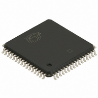
CY7C4245-10ASXC Cypress Semiconductor Corp, CY7C4245-10ASXC Datasheet - Page 10

CY7C4245-10ASXC
Manufacturer Part Number
CY7C4245-10ASXC
Description
IC SYNC FIFO MEM 4KX18 64LQFP
Manufacturer
Cypress Semiconductor Corp
Series
CY7Cr
Datasheet
1.CY7C4245-15JXC.pdf
(22 pages)
Specifications of CY7C4245-10ASXC
Function
Synchronous
Memory Size
72K (4K x 18)
Data Rate
100MHz
Access Time
8ns
Voltage - Supply
3.3V
Operating Temperature
-40°C ~ 85°C
Mounting Type
Surface Mount
Package / Case
64-LQFP
Lead Free Status / RoHS Status
Lead free / RoHS Compliant
Available stocks
Company
Part Number
Manufacturer
Quantity
Price
Company:
Part Number:
CY7C4245-10ASXC
Manufacturer:
Cypress Semiconductor Corp
Quantity:
10 000
Company:
Part Number:
CY7C4245-10ASXCT
Manufacturer:
Cypress Semiconductor Corp
Quantity:
10 000
Switching Characteristics
Switching Waveforms
Note
Document Number: 001-45652 Rev. **
t
t
t
t
t
t
t
18. t
HF
XO
XI
XIS
SKEW1
SKEW2
SKEW3
Parameter
the rising edge of RCLK and the rising edge of WCLK is less than t
SKEW1
WCLK
RCLK
–D
WEN
REN
FF
17
is the minimum time between a rising RCLK edge and a rising WCLK edge to guarantee that FF will go HIGH during the current clock cycle. If the time between
Clock to Half-Full Flag
Clock to Expansion Out
Expansion in Pulse Width
Expansion in Set-up Time
Skew Time between Read Clock and Write Clock
for Full Flag
Skew Time between Read Clock and Write Clock
for Empty Flag
Skew Time between Read Clock and Write Clock
for Programmable Almost Empty and Program-
mable Almost Full Flags.
t
SKEW1
Description
Over the Operating Range (continued)
t
[18]
CLKH
t
WFF
t
CLK
Figure 6. Write Cycle Timing
t
DS
SKEW1
t
CLKL
t
ENS
, then FF may not change state until the next WCLK edge.
Min.
4.5
10
3
5
5
-10
Max.
t
DH
12
t
ENH
7
t
WFF
Min.
6.5
15
5
6
6
-15
Max.
16
10
NO OPERATION
CY7C4425/4205/4215
CY7C4225/4235/4245
Min.
10
10
10
10
18
-25
Max.
20
15
Min.
14
15
12
12
20
-35
Page 10 of 22
Max.
25
20
Unit
ns
ns
ns
ns
ns
ns
ns
[+] Feedback


