74ABT16541CSSCX Fairchild Semiconductor, 74ABT16541CSSCX Datasheet - Page 4
74ABT16541CSSCX
Manufacturer Part Number
74ABT16541CSSCX
Description
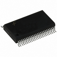
IC BUFF DVR TRI-ST 16BIT 48SSOP
Manufacturer
Fairchild Semiconductor
Series
74ABTr
Datasheet
1.74ABT16541CMTD.pdf
(8 pages)
Specifications of 74ABT16541CSSCX
Logic Type
Buffer/Line Driver, Non-Inverting
Number Of Elements
2
Number Of Bits Per Element
8
Current - Output High, Low
32mA, 64mA
Voltage - Supply
4.5 V ~ 5.5 V
Operating Temperature
-40°C ~ 85°C
Mounting Type
Surface Mount
Package / Case
48-SSOP
Lead Free Status / RoHS Status
Lead free / RoHS Compliant
Available stocks
Company
Part Number
Manufacturer
Quantity
Price

Part Number:
74ABT16541CSSCX
Manufacturer:
FAIRCHILD/仙童
Quantity:
20 000


www.fairchildsemi.com
f
t
t
t
t
t
t
V
t
t
t
t
t
t
TOGGLE
PLH
PHL
PZH
PZL
PHZ
PLZ
DC Electrical Characteristics
Symbol
Note 3: Guaranteed but not tested.
Note 4: Max number of outputs defined as (n). n-1 data inputs are driven 0V to 3V. One output at LOW. Guaranteed, but not tested.
Note 5: Max number of data inputs (n) switching. n-1 inputs switching 0V to 3V. Input-under-test switching: 3V to threshold (V
Guaranteed, but not tested.
Note 6: Max number of outputs defined as (n). n
AC Electrical Characteristics
Extended AC Electrical Characteristics
Note 7: This specification is guaranteed but not tested. The limits apply to propagation delays for all paths described switching in phase
(i.e., all LOW-to-HIGH, HIGH-to-LOW, etc.).
Note 8: This specification is guaranteed but not tested. The limits represent propagation delay with 250 pF load capacitors in place of the 50 pF load capac-
itors in the standard AC load. This specification pertains to single output switching only.
Note 9: This specification is guaranteed but not tested. The limits represent propagation delays for all paths described switching in phase
(i.e., all LOW-to-HIGH, HIGH-to-LOW, etc.) with 250 pF load capacitors in place of the 50 pF load capacitors in the standard AC load.
Note 10: The 3-STATE delay times are dominated by the RC network (500
PLH
PHL
PZH
PZL
PHZ
PLZ
ILD
Symbol
Symbol
Maximum LOW Level Dynamic Input Voltage
Maximum Toggle Frequency
Propagation Delay
Data to Outputs
Output Enable
Time
Output Disable
Time
Propagation
Delay Data to Outputs
Output Enable
Time
Output Disable
Time
Parameter
Parameter
Parameter
1 data inputs are driven 0V to 3V. One output HIGH. Guaranteed, but not tested.
Min
1.5
1.5
1.5
1.5
1.0
1.0
16 Outputs Switching
V
(Continued)
CC
40
C
q
(Note 7)
L
Min
C to
Min
4.5V–5.5V
1.0
1.0
1.5
1.5
1.0
1.0
Typ
100
50 pF
:
85
, 250 pF) on the output and have been excluded from the datasheet.
4
q
C
Typ
1.2
C
T
V
L
A
Max
CC
5.0
5.3
6.5
6.5
6.7
6.7
Typ
2.3
3.5
3.5
4.2
3.2
2.7
50 pF
25
5V
q
C
Max
0.8
T
1 Output Switching
A
V
Min
1.5
1.5
2.5
2.5
CC
C
Max
3.4
3.9
5.2
6.0
5.1
5.1
(Note 10)
L
(Note 8)
40
Units
4.5V–5.5V
q
250 pF
C to
V
Max
6.0
6.0
7.8
7.8
85
T
q
A
Min
C
V
1.0
1.0
1.5
1.5
1.0
1.0
V
5.0
CC
CC
C
40
L
16 Outputs Switching
T
4.5V–5.5V
q
A
V
C to
Min
T
50 pF
2.5
2.5
2.5
2.5
ILD
CC
A
C
), 0V to threshold (V
L
(Note 10)
40
(Note 9)
25
Max
85
3.4
3.9
5.2
6.0
5.1
5.1
4.5V–5.5V
q
250 pF
C to
q
q
C (Note 5)
Conditions
C
Max
8.0
8.0
9.5
8.5
85
q
C
Units
ns
ns
ns
IHD
Units
MHz
ns
ns
ns
).
Related parts for 74ABT16541CSSCX
Image
Part Number
Description
Manufacturer
Datasheet
Request
R

Part Number:
Description:
Fairchild Semiconductor [IGBT MODULE]
Manufacturer:
Fairchild Semiconductor
Datasheet:

Part Number:
Description:
Discrete Semiconductor Modules
Manufacturer:
Fairchild Semiconductor
Part Number:
Description:
Discrete Semiconductor Modules
Manufacturer:
Fairchild Semiconductor
Part Number:
Description:
This N-Channel MOSFET is produced using Fairchild Semiconductor’s advanced Power Trench® process
Manufacturer:
Fairchild Semiconductor
Datasheet:
Part Number:
Description:
This N-Channel MOSFET is produced using Fairchild Semiconductor’s advanced Power Trench® process
Manufacturer:
Fairchild Semiconductor
Datasheet:
Part Number:
Description:
This N-Channel MOSFET is produced using Fairchild Semiconductor’s advanced PowerTrench® process
Manufacturer:
Fairchild Semiconductor
Datasheet:
Part Number:
Description:
This N-Channel MOSFET is produced using Fairchild Semiconductor’s advanced PowerTrench® process
Manufacturer:
Fairchild Semiconductor
Datasheet:
Part Number:
Description:
This N-Channel MOSFET is produced using Fairchild Semiconductor’s advanced Power Trench® process
Manufacturer:
Fairchild Semiconductor
Datasheet:
Part Number:
Description:
This N-Channel logic Level MOSFETs are produced using Fairchild Semiconductor‘s advanced Power Trench® process that has been special tailored to minimize the on-state resistance and yet maintain superior switching performance
Manufacturer:
Fairchild Semiconductor
Datasheet:
Part Number:
Description:
This N-Channel MOSFET is produced using Fairchild Semiconductor’s advanced Power Trench® process
Manufacturer:
Fairchild Semiconductor
Datasheet:
Part Number:
Description:
This N-Channel SyncFET™ is produced using Fairchild Semiconductor’s advanced PowerTrench® process
Manufacturer:
Fairchild Semiconductor
Datasheet:
Part Number:
Description:
This N-Channel SyncFET™ is produced using Fairchild Semiconductor’s advanced PowerTrench® process
Manufacturer:
Fairchild Semiconductor
Datasheet:
Part Number:
Description:
This N-Channel SyncFET™ is produced using Fairchild Semiconductor’s advanced PowerTrench® process
Manufacturer:
Fairchild Semiconductor
Datasheet:
Part Number:
Description:
This N-Channel logic Level MOSFETs are produced using Fairchild Semiconductor‘s advanced Power Trench® process that has been special tailored to minimize the on-state resistance and yet maintain superior switching performance
Manufacturer:
Fairchild Semiconductor
Datasheet:
Part Number:
Description:
This N-Channel MOSFET is produced using Fairchild Semiconductor’s advanced Power Trench® process that has been especially tailored to minimize the on-state resistance and yet maintain superior switching performance
Manufacturer:
Fairchild Semiconductor
Datasheet: