74LVX125MX Fairchild Semiconductor, 74LVX125MX Datasheet - Page 2
74LVX125MX
Manufacturer Part Number
74LVX125MX
Description
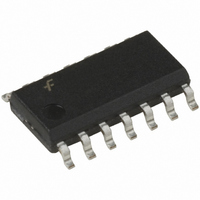
IC BUFFER TRI-ST QD LOW V 14SOIC
Manufacturer
Fairchild Semiconductor
Series
74LVXr
Datasheet
1.74LVX125SJX.pdf
(8 pages)
Specifications of 74LVX125MX
Logic Type
Buffer/Line Driver, Non-Inverting
Number Of Elements
4
Number Of Bits Per Element
1
Current - Output High, Low
4mA, 4mA
Voltage - Supply
2 V ~ 3.6 V
Operating Temperature
-40°C ~ 85°C
Mounting Type
Surface Mount
Package / Case
14-SOIC (3.9mm Width), 14-SOL
Logic Family
LVX
Number Of Channels Per Chip
4
Polarity
Non-Inverting
Supply Voltage (max)
3.6 V
Supply Voltage (min)
2 V
Maximum Operating Temperature
+ 85 C
Mounting Style
SMD/SMT
High Level Output Current
- 4 mA
Low Level Output Current
4 mA
Maximum Power Dissipation
180 mW
Minimum Operating Temperature
- 40 C
Number Of Lines (input / Output)
4 / 3
Output Type
3-State
Propagation Delay Time
13.6 ns at 2.7 V, 9.7 ns at 3.3 V
Lead Free Status / RoHS Status
Lead free / RoHS Compliant
Available stocks
Company
Part Number
Manufacturer
Quantity
Price
Company:

Part Number:
74LVX125MX
Manufacturer:
MAXIM
Quantity:
500
Part Number:
74LVX125MX
Manufacturer:
FAIRCHILD/仙童
Quantity:
20 000


©1994 Fairchild Semiconductor Corporation
74LVX125 Rev. 1.4.0
Absolute Maximum Ratings
Stresses exceeding the absolute maximum ratings may damage the device. The device may not function or be
operable above the recommended operating conditions and stressing the parts to these levels is not recommended.
In addition, extended exposure to stresses above the recommended operating conditions may affect device reliability.
The absolute maximum ratings are stress ratings only.
Recommended Operating Conditions
The Recommended Operating Conditions table defines the conditions for actual device operation. Recommended
operating conditions are specified to ensure optimal performance to the datasheet specifications. Fairchild does not
recommend exceeding them or designing to absolute maximum ratings.
Note:
1. Unused inputs must be held HIGH or LOW. They may not float.
I
CC
Symbol
Symbol
T
V
V
or I
t / V
I
V
V
I
STG
V
OK
I
T
V
P
CC
IK
O
CC
O
O
A
I
I
GND
Supply Voltage
DC Input Diode Current, V
DC Input Voltage
DC Output Diode Current
DC Output Voltage
DC Output Source or Sink Current
DC V
Storage Temperature
Power Dissipation
Supply Voltage
Input Voltage
Output Voltage
Operating Temperature
Input Rise and Fall Time
V
V
O
O
CC
V
–0.5V
or Ground Current
CC
+ 0.5V
I
–0.5V
Parameter
Parameter
(1)
2
–0.5V to V
Rating
Rating
–65°C to +150°C
0ns/V to 100ns/V
–40°C to +85°C
–0.5V to +7.0V
www.fairchildsemi.com
2.0V to 3.6V
–0.5V to 7V
0V to 5.5V
CC
0V to V
180mW
–20mA
–20mA
+20mA
±25mA
±50mA
+ 0.5V
CC
Related parts for 74LVX125MX
Image
Part Number
Description
Manufacturer
Datasheet
Request
R

Part Number:
Description:
TXRX 8BIT DUAL CONF VOLT 24TSSOP
Manufacturer:
Fairchild Semiconductor
Datasheet:

Part Number:
Description:
TXRX 8BIT DUAL CONF VOLT 24SOIC
Manufacturer:
Fairchild Semiconductor
Datasheet:

Part Number:
Description:
TXRX 8BIT DUAL CONF VOLT 24QSOP
Manufacturer:
Fairchild Semiconductor
Datasheet:
Part Number:
Description:
TXRX 8BIT DUAL CONF VOLT 24QSOP
Manufacturer:
Fairchild Semiconductor
Datasheet:

Part Number:
Description:
IC SWITCH QUAD 1X2 14TSSOP
Manufacturer:
NXP Semiconductors
Datasheet:

Part Number:
Description:
IC MUX/DEMUX DUAL 4X1 16SSOP
Manufacturer:
NXP Semiconductors
Datasheet:

Part Number:
Description:
IC MUX/DEMUX 8X1 16TSSOP
Manufacturer:
NXP Semiconductors
Datasheet:
Part Number:
Description:
IC MUX/DEMUX DUAL 4X1 16TSSOP
Manufacturer:
NXP Semiconductors
Datasheet:
Part Number:
Description:
IC MUX/DEMUX TRIPLE 2X1 16TSSOP
Manufacturer:
NXP Semiconductors
Datasheet:

Part Number:
Description:
IC MUX/DEMUX 8X1 16SOIC
Manufacturer:
NXP Semiconductors
Datasheet:
Part Number:
Description:
IC MUX/DEMUX 8X1 16SSOP
Manufacturer:
NXP Semiconductors
Datasheet:
Part Number:
Description:
IC MUX/DEMUX DUAL 4X1 16SOIC
Manufacturer:
NXP Semiconductors
Datasheet:
Part Number:
Description:
IC MUX/DEMUX TRIPLE 2X1 16SOIC
Manufacturer:
NXP Semiconductors
Datasheet:
Part Number:
Description:
IC MUX/DEMUX TRIPLE 2X1 16SSOP
Manufacturer:
NXP Semiconductors
Datasheet:

Part Number:
Description:
IC SWITCH QUAD 1X2 14SOIC
Manufacturer:
NXP Semiconductors
Datasheet: