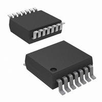
ISL55141IVZ Intersil, ISL55141IVZ Datasheet - Page 7

ISL55141IVZ
Manufacturer Part Number
ISL55141IVZ
Description
IC COMP CMOS HS 18V 14-TSSOP
Manufacturer
Intersil
Type
Windowr
Datasheet
1.ISL55141IVZ.pdf
(14 pages)
Specifications of ISL55141IVZ
Number Of Elements
1
Voltage - Supply
10 V ~ 18 V
Mounting Type
Surface Mount
Package / Case
14-TSSOP
Lead Free Status / RoHS Status
Lead free / RoHS Compliant
Available stocks
Company
Part Number
Manufacturer
Quantity
Price
Company:
Part Number:
ISL55141IVZ
Manufacturer:
SEAGATE
Quantity:
100
Part Number:
ISL55141IVZ
Manufacturer:
INTERSIL
Quantity:
20 000
The maximum power dissipation allowed in a package is
determined according to Equation 1.
where:
• T
• T
• θ
• P
Approximate Power Dissipation
(Typ) P = N*[(V
CL*(V
where:
N is the number of comparators in the chip
(1 for ISL55141, 2 for ISL55142 and 4 for ISL55143).
(f) is the operating frequency.
CL is the load capacitor.
The power dissipation calculated from the above formula
may have an error of ±20 to 25%.
The maximum power dissipation actually produced by an IC
is the total quiescent supply current times the total power
supply voltage, plus the power in the IC due to the loads.
Power also depends on the number of channels changing
state and frequency of operation. The extent of continuous
active pattern generation/reception will greatly affect
dissipation requirements.
The user should evaluate various heat sink/cooling options
in order to control the ambient temperature part of the
equation. This is especially true if the user’s applications
require continuous, high-speed operation.
Note: The reader is cautioned against assuming the same
level of thermal performance in actual applications. A careful
inspection of conditions in your application should be
conducted.
P
DMAX
AMAX
JA
JMAX
DMAX
OH
= Thermal resistance of the package
=
-V
= Maximum junction temperature
= Maximum ambient temperature
T
-------------------------------------------- -
= Maximum power dissipation in the package
OL
JMAX
)^2*f]
CC
Θ
- T
JA
-V
AMAX
EE
)*8.25mW + 90pF*(V
7
ISL55141, ISL55142, ISL55143
CC
-V
EE
)^2*f +
(EQ. 1)
Power Supply Information
Circuit design must always take into account the internal
EOS/ESD protection structure of the device.
Important Note: The QFN package metal plane is used
for heat sinking of the device. It is electrically connected
to the negative supply potential (V
ground, the thermal pad can be connected to ground.
Otherwise, the thermal pad (V
other power planes.
Power Supply Sequencing
The ISL55141, ISL55142, ISL55143 reference every supply
with respect to V
followed by the CV
V
In cases where inputs may exceed voltage rails during
power-up, series resistance should be employed to
safeguard EOS to the ESD protection diodes.
INP
CV
CV
V
INP
B
pin should not exceed V
A
EE
A
. Therefore, apply V
and CV
V
V
B
EE
CC
EE
supplies. The comparator
EE
or V
) must be isolated from
OPTIONAL PROTECTION
DIODE
OPTIONAL PROTECTION
DIODE
EE
CC
EE
). If V
during power-up.
, V
OL
EE
then V
is tied to
V
V
March 1, 2011
OH
OL
Q
Q
FN6230.2
CC
B
A


