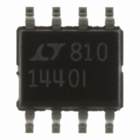
LTC1440IS8 Linear Technology, LTC1440IS8 Datasheet - Page 11

LTC1440IS8
Manufacturer Part Number
LTC1440IS8
Description
IC COMP W/REF LP SINGLE 8-SOIC
Manufacturer
Linear Technology
Type
with Voltage Referencer
Datasheet
1.LTC1440CS8PBF.pdf
(16 pages)
Specifications of LTC1440IS8
Number Of Elements
1
Output Type
CMOS, TTL
Voltage - Supply
2 V ~ 11 V, ±1 V ~ 5.5 V
Mounting Type
Surface Mount
Package / Case
8-SOIC (0.154", 3.90mm Width)
Lead Free Status / RoHS Status
Contains lead / RoHS non-compliant
Available stocks
Company
Part Number
Manufacturer
Quantity
Price
Company:
Part Number:
LTC1440IS8
Manufacturer:
LT
Quantity:
10 000
Part Number:
LTC1440IS8
Manufacturer:
LINEAR/凌特
Quantity:
20 000
Company:
Part Number:
LTC1440IS8#TRPBF
Manufacturer:
PHI
Quantity:
6 230
APPLICATIONS
Hysteresis
Hysteresis can be added to the LTC1440 by connecting a
resistor (R1) between the REF and HYST pins and a
second resistor (R2) from HYST to V
The difference between the upper and lower threshold
voltages, or hysteresis voltage band (V
the voltage difference between the REF and HYST pins.
When more hysteresis is added, the upper threshold
increases the same amount as the low threshold de-
creases. The maximum voltage allowed between REF and
HYST pins is 50mV, producing a maximum hysteresis
voltage band of 100mV. The hysteresis band could vary by
5V
TO
8V
Figure 3a. Reference Transient Response Test Circuit
V
Figure 3b. Reference and Comparator Output
Transient Response
+
V
OUT
REF
8V
5V
R3
2.4M
10k
R2
U
R1
430Ω
C1
1µF
INFORMATION
3
4
5
6
U
2ms/DIV
IN
IN
HYST
REF
+
–
V
2
+
–
–
W
V
+
HB
LTC1440
7
–
(Figure 4).
GND
), is equal to twice
1440/1/2 F03b
1
U
8
1440/1/2 F03a
OUT
up to 15%. If hysteresis is not wanted, the HYST pin
should be shorted to REF. Acceptable values for I
from 0.1µA to 5µA. If 2.4M is chosen for R2, then the value
of R1 is equal to the value of V
Level Detector
The LTC1440 is ideal for use as a micropower level
detector as shown in Figure 5. R1 and R2 form a voltage
divider from V
and R4 set the hysteresis voltage, and R5 and C1 bypass
the reference output. The following design procedure can
be used to select the component values:
1. Choose the V
V
IN
Figure 5. Glitch-Free Level Detector with Hysteresis
R2
3.4M
1%
R1
1.18M
1%
LTC1440/LTC1441/LTC1442
I
REF
R4
2.4M
1%
Figure 4. Programmable Hysteresis
R1
R2
15k
1%
IN
R3
IN
to the noninverting comparator input. R3
voltage trip level, in this example 4.65V.
6
5
R5
430Ω
5%
REF
HYST
C1
1µF
3
4
5
6
LTC1440
V
IN
IN
HYST
REF
–
2
+
–
HB
V
2
+
–
–
.
5V
V
R1 =
R2 =
+
LTC1440
7
GND
(2)(I
(
1.182V –
V
1
HB
REF
I
REF
1440/1/2 F04
)
V
1440/1/2 F05
8
2
HB
REF
)
11
OUT
range
144012fd


