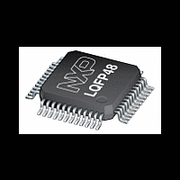
MPT612 NXP Semiconductors, MPT612 Datasheet - Page 22

MPT612
Manufacturer Part Number
MPT612
Description
The MPT612, the first dedicated IC for performing the Maximum Power Point Tracking (MPPT) function, is designed for use in applications that use solar photovoltaic (PV) cells or in fuel cells
Manufacturer
NXP Semiconductors
Datasheet
1.MPT612.pdf
(37 pages)
Available stocks
Company
Part Number
Manufacturer
Quantity
Price
Company:
Part Number:
MPT612FBD48,151
Manufacturer:
ON
Quantity:
22 150
Company:
Part Number:
MPT612FBD48,151
Manufacturer:
NXP Semiconductors
Quantity:
10 000
NXP Semiconductors
[1]
[2]
[3]
[4]
[5]
[6]
[7]
[8]
[9]
[10] Accounts for 100 mV voltage drop in all supply lines.
[11] Allowed as long as the current limit does not exceed the maximum current allowed by the device.
[12] Minimum condition for V
[13] Applies to PIO25:16.
[14] Battery supply current on pin V
[15] Input leakage current to GND.
Table 5.
V
[1]
[2]
[3]
[4]
[5]
[6]
[7]
MPT612
Product data sheet
Symbol
Oscillator pins
V
V
V
V
Symbol
V
C
E
E
E
E
E
DD(ADC)
i(XTAL1)
o(XTAL2)
i(RTCX1)
o(RTCX2)
IA
ia
D
L(adj)
O
G
T
Typical ratings are not guaranteed. The values listed are at room temperature (25 °C), nominal supply voltages.
Core and internal rail.
External rail.
If V
If V
The RTC typically fails when V
Including voltage on outputs in 3-state mode.
V
3-state outputs go into 3-state mode when V
Conditions: GNDADC = 0 V, V
8-bit resolution at full speed.
The ADC is monotonic, there are no missing codes.
The differential linearity error (E
The integral non-linearity (E
appropriate adjustment of gain and offset errors. See
The offset error (E
ideal curve. See
The gain error (E
error and the straight line which fits the ideal transfer curve. See
The absolute error (E
ADC and the ideal transfer curve. See
DD(IO)
DD(IO)
DD(ADC)
= 2.5 V to 3.6 V; T
supply voltages must be present.
Parameter
input voltage on pin
XTAL1
output voltage on pin
XTAL2
input voltage on pin
RTCX1
output voltage on pin
RTCX2
< 3.0 V, the I/O pins are not 5 V tolerant and the ADC input voltage is limited to V
ADC Static Characteristics
< 3.0 V, the I/O pins are not 5 V tolerant.
Parameter
analog input voltage
analog input capacitance
differential linearity error
integral non-linearity
offset error
gain error
absolute error
Fig 4.
G
) is the relative difference in percent between the straight line fitting the actual transfer curve after removing offset
O
) is the absolute difference between the straight line which fits the actual curve and the straight line which fits the
T
) is the maximum difference between the center of the steps of the actual transfer curve of the non-calibrated
I
amb
= 4.5 V, maximum condition for V
L(adj)
= -40
DD(ADC)
DD(RTC)
DD(RTC)
) is the peak difference between the center of the steps of the actual and the ideal transfer curve after
D
) is the difference between the actual step width and the ideal step width. See
Conditions
°
C to +85
.
= 3.3 V and V
drops below 1.6 V.
Fig 4.
All information provided in this document is subject to legal disclaimers.
DD(IO)
°
C unless otherwise specified. ADC frequency 4.5 MHz
is grounded.
Rev. 2 — 14 September 2010
DD(IO)
Conditions
Fig 4.
= 3.3 V for 10-bit resolution at full speed; V
I
= 5.5 V. V
Fig 4.
DD(ADC)
≥ 3 .0 V and V
[1][2][3]
[1][2][4]
[1][5]
[1][6]
[1][7]
Min
0
0
0
0
Min
0
-
-
-
-
-
-
Maximum power point tracking IC
DD(ADC)
DD(IO)
≥ 3 .0 V.
= 3.0 V.
DD(ADC)
Typ
-
-
-
-
Typ
-
-
-
-
-
-
-
= 2.6 V, V
Fig 4.
© NXP B.V. 2010. All rights reserved.
MPT612
Max
V
1
±1
±2
±3
±0.5
±4
DD(IO)
Max
DD(ADC)
1.8
1.8
1.8
1.8
= 2.6 V for
Unit
V
pF
LSB
LSB
LSB
%
LSB
22 of 22
Unit
V
V
V
V


