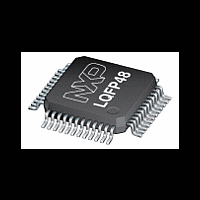
LPC11C12FBD48 NXP Semiconductors, LPC11C12FBD48 Datasheet - Page 14

LPC11C12FBD48
Manufacturer Part Number
LPC11C12FBD48
Description
The LPC11C12FBD48 is an ARM Cortex-M0 microcontroller designed for 8/16-bit microcontroller applications, offering performance, low power, simple instruction set and memory addressing together with reduced code size compared to existing 8/16-bit arch
Manufacturer
NXP Semiconductors
Datasheet
1.LPC11C12FBD48.pdf
(62 pages)
Available stocks
Company
Part Number
Manufacturer
Quantity
Price
Company:
Part Number:
LPC11C12FBD48
Manufacturer:
VISHAY
Quantity:
2 462
Company:
Part Number:
LPC11C12FBD48/301
Manufacturer:
NXP
Quantity:
5 000
Company:
Part Number:
LPC11C12FBD48/301,
Manufacturer:
NXP Semiconductors
Quantity:
10 000
NXP Semiconductors
Table 4.
[1]
[2]
[3]
[4]
[5]
[6]
[7]
LPC11CX2_CX4
Product data sheet
Symbol
GND
V
XTALIN
XTALOUT
V
DD
SS
Pin state at reset for default function: I = Input; O = Output; PU = internal pull-up enabled (pins pulled up to full V
no pull-up/down enabled.
See
reset the chip and wake up from Deep power-down mode. An external pull-up resistor is required on this pin for the Deep power-down
mode.
5 V tolerant pad providing digital I/O functions with configurable pull-up/pull-down resistors and configurable hysteresis (see
I
5 V tolerant pad providing digital I/O functions with configurable pull-up/pull-down resistors, configurable hysteresis, and analog input.
When configured as a ADC input, digital section of the pad is disabled and the pin is not 5 V tolerant (see
5 V tolerant digital I/O pad without pull-up/pull-down resistors.
When the system oscillator is not used, connect XTALIN and XTALOUT as follows: XTALIN can be left floating or can be grounded
(grounding is preferred to reduce susceptibility to noise). XTALOUT should be left floating.
2
C-bus pads compliant with the I
Figure 26
LPC11C22/C24 pin description table
for reset pad configuration. RESET functionality is not available in Deep power-down mode. Use the WAKEUP pin to
Pin
21
8; 44
6
7
5; 41
[7]
[7]
Start
logic
inputs
-
-
-
-
-
2
C-bus specification for I
Type
-
I
I
O
I
All information provided in this document is subject to legal disclaimers.
Reset
state
[1]
-
-
-
-
-
Rev. 3 — 27 June 2011
Ground for CAN transceiver.
Supply voltage to the internal regulator, the external rail, and the
Ground.
Description
ADC. Also used as the ADC reference voltage.
Input to the oscillator circuit and internal clock generator circuits.
Input voltage must not exceed 1.8 V.
Output from the oscillator amplifier.
2
C standard mode and I
2
C Fast-mode Plus.
32-bit ARM Cortex-M0 microcontroller
LPC11Cx2/Cx4
Figure
DD
© NXP B.V. 2011. All rights reserved.
25).
level); IA = inactive,
Figure
14 of 62
25).


