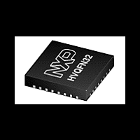
LPC1114FHI33 NXP Semiconductors, LPC1114FHI33 Datasheet - Page 20

LPC1114FHI33
Manufacturer Part Number
LPC1114FHI33
Description
The LPC1114FHI33 is an ARM Cortex-M0 microcontroller and it can operate up to 50 MHz
Manufacturer
NXP Semiconductors
Datasheet
1.LPC1110FD20.pdf
(103 pages)
- Current page: 20 of 103
- Download datasheet (2Mb)
NXP Semiconductors
Table 7.
[1]
[2]
[3]
[4]
[5]
Table 8.
LPC111X
Product data sheet
Symbol
XTALOUT
V
V
Symbol
PIO0_0 to PIO0_11
RESET/PIO0_0
PIO0_1/CLKOUT/
CT32B0_MAT2
PIO0_2/SSEL0/
CT16B0_CAP0
PIO0_3
PIO0_4/SCL
SS
SSA
Pin state at reset for default function: I = Input; O = Output; PU = internal pull-up enabled (pins pulled up to full V
no pull-up/down enabled.
See
reset the chip and wake up from Deep power-down mode. An external pull-up resistor is required on this pin for the Deep power-down
mode.
5 V tolerant pad providing digital I/O functions with configurable pull-up/pull-down resistors and configurable hysteresis (see
5 V tolerant pad providing digital I/O functions with configurable pull-up/pull-down resistors, configurable hysteresis, and analog input.
When configured as a ADC input, digital section of the pad is disabled and the pin is not 5 V tolerant (see
When the system oscillator is not used, connect XTALIN and XTALOUT as follows: XTALIN can be left floating or can be grounded
(grounding is preferred to reduce susceptibility to noise). XTALOUT should be left floating.
Figure 46
LPC1100L series: LPC1112 pin description table (TSSOP20 with V
LPC1100L series: LPC1112/14 pin description table (TSSOP28 and DIP28 packages)
for the reset pad configuration. RESET functionality is not available in Deep power-down mode. Use the WAKEUP pin to
13
16
6
23
24
25
26
27
[5]
[2]
[3]
[3]
[3]
[4]
Start
logic
input
-
-
-
Start
logic
input
yes
yes
yes
yes
yes
Type Reset
I/O
I
I/O
I/O
O
O
I/O
I/O
I
I/O
I/O
I/O
All information provided in this document is subject to legal disclaimers.
Type
O
I
I
state
[1]
I; PU
-
I; PU
-
-
I; PU
-
-
I; PU
I; IA
-
Rev. 7 — 1 March 2012
Reset
state
[1]
-
-
-
Description
Port 0 — Port 0 is a 12-bit I/O port with individual direction and
function controls for each bit. The operation of port 0 pins depends
on the function selected through the IOCONFIG register block.
RESET — External reset input with 20 ns glitch filter. A LOW-going
pulse as short as 50 ns on this pin resets the device, causing I/O
ports and peripherals to take on their default states, and processor
execution to begin at address 0.
PIO0_0 — General purpose digital input/output pin with 10 ns
glitch filter.
PIO0_1 — General purpose digital input/output pin. A LOW level
on this pin during reset starts the ISP command handler.
CLKOUT — Clockout pin.
CT32B0_MAT2 — Match output 2 for 32-bit timer 0.
PIO0_2 — General purpose digital input/output pin.
SSEL0 — Slave Select for SPI0.
CT16B0_CAP0 — Capture input 0 for 16-bit timer 0.
PIO0_3 — General purpose digital input/output pin.
PIO0_4 — General purpose digital input/output pin (open-drain).
SCL — I
only if I
register.
Description
Output from the oscillator amplifier.
Ground.
Analog ground.
2
C Fast-mode Plus is selected in the I/O configuration
2
C-bus, open-drain clock input/output. High-current sink
LPC1110/11/12/13/14/15
32-bit ARM Cortex-M0 microcontroller
DDA
and V
SSA
pins)
Figure
…continued
DD
© NXP B.V. 2012. All rights reserved.
45).
level ); IA = inactive,
Figure
20 of 103
45).
Related parts for LPC1114FHI33
Image
Part Number
Description
Manufacturer
Datasheet
Request
R

Part Number:
Description:
MCU, MPU & DSP Development Tools LPC1114 Demo Boards Cortex M0
Manufacturer:
NXP Semiconductors
Datasheet:
Part Number:
Description:
LPC1114FBD48/LQFP48/REEL13//30
Manufacturer:
NXP Semiconductors
Datasheet:
Part Number:
Description:
NXP Semiconductors designed the LPC2420/2460 microcontroller around a 16-bit/32-bitARM7TDMI-S CPU core with real-time debug interfaces that include both JTAG andembedded trace
Manufacturer:
NXP Semiconductors
Datasheet:

Part Number:
Description:
NXP Semiconductors designed the LPC2458 microcontroller around a 16-bit/32-bitARM7TDMI-S CPU core with real-time debug interfaces that include both JTAG andembedded trace
Manufacturer:
NXP Semiconductors
Datasheet:
Part Number:
Description:
NXP Semiconductors designed the LPC2468 microcontroller around a 16-bit/32-bitARM7TDMI-S CPU core with real-time debug interfaces that include both JTAG andembedded trace
Manufacturer:
NXP Semiconductors
Datasheet:
Part Number:
Description:
NXP Semiconductors designed the LPC2470 microcontroller, powered by theARM7TDMI-S core, to be a highly integrated microcontroller for a wide range ofapplications that require advanced communications and high quality graphic displays
Manufacturer:
NXP Semiconductors
Datasheet:
Part Number:
Description:
NXP Semiconductors designed the LPC2478 microcontroller, powered by theARM7TDMI-S core, to be a highly integrated microcontroller for a wide range ofapplications that require advanced communications and high quality graphic displays
Manufacturer:
NXP Semiconductors
Datasheet:
Part Number:
Description:
The Philips Semiconductors XA (eXtended Architecture) family of 16-bit single-chip microcontrollers is powerful enough to easily handle the requirements of high performance embedded applications, yet inexpensive enough to compete in the market for hi
Manufacturer:
NXP Semiconductors
Datasheet:
Part Number:
Description:
The XA-S3 device is a member of Philips Semiconductors? XA(eXtended Architecture) family of high performance 16-bitsingle-chip microcontrollers
Manufacturer:
NXP Semiconductors
Datasheet:

Part Number:
Description:
The NXP BlueStreak LH75401/LH75411 family consists of two low-cost 16/32-bit System-on-Chip (SoC) devices
Manufacturer:
NXP Semiconductors
Datasheet:

Part Number:
Description:
The NXP LPC3130/3131 combine an 180 MHz ARM926EJ-S CPU core, high-speed USB2
Manufacturer:
NXP Semiconductors
Datasheet:

Part Number:
Description:
The NXP LPC3141 combine a 270 MHz ARM926EJ-S CPU core, High-speed USB 2
Manufacturer:
NXP Semiconductors

Part Number:
Description:
The NXP LPC3143 combine a 270 MHz ARM926EJ-S CPU core, High-speed USB 2
Manufacturer:
NXP Semiconductors

Part Number:
Description:
The NXP LPC3152 combines an 180 MHz ARM926EJ-S CPU core, High-speed USB 2
Manufacturer:
NXP Semiconductors


