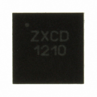
ZXCD1210JB16TA Diodes Zetex, ZXCD1210JB16TA Datasheet - Page 2

ZXCD1210JB16TA
Manufacturer Part Number
ZXCD1210JB16TA
Description
IC AMP AUDIO CLASS D 16QFN
Manufacturer
Diodes Zetex
Type
Modulatorr
Datasheet
1.ZXCD1210JB16TA.pdf
(8 pages)
Specifications of ZXCD1210JB16TA
Applications
Multimedia
Mounting Type
Surface Mount
Package / Case
16-QFN
Operational Class
Class-D
Audio Amplifier Output Configuration
1-Channel Mono
Audio Amplifier Function
Speaker
Total Harmonic Distortion
0.05%
Single Supply Voltage (typ)
16V
Dual Supply Voltage (typ)
Not RequiredV
Power Supply Requirement
Single
Power Dissipation
1W
Rail/rail I/o Type
No
Single Supply Voltage (min)
12V
Single Supply Voltage (max)
18V
Dual Supply Voltage (min)
Not RequiredV
Dual Supply Voltage (max)
Not RequiredV
Operating Temp Range
-40C to 70C
Operating Temperature Classification
Commercial
Mounting
Surface Mount
Pin Count
16
Package Type
QFN
Lead Free Status / RoHS Status
Lead free / RoHS Compliant
Other names
ZXCD1210JB16TR
Available stocks
Company
Part Number
Manufacturer
Quantity
Price
Company:
Part Number:
ZXCD1210JB16TA
Manufacturer:
ZETEX
Quantity:
1 000
Absolute maximum ratings
V
Power dissipation
Package thermal resistance ( ja)
Operating temperature range
Maximum junction temperature
Storage temperature range
Stresses beyond those listed under ‘Absolute maximum ratings’ may cause permanent damage to the device. These are
stress ratings only, and functional operation of the device at these or any other conditions beyond those indicated in the
operational sections of the specifications is not implied. Exposure to absolute maximum conditions for extended periods
may affect device reliability.
Electrical characteristics
(*) For optimum thermal performance it is recommended that the ZXCD1210 is operated with a V
Issue 2 - October 2007
© Zetex Semiconductors plc 2007
NOTES:
Symbol Parameter
V
I
F
T
V
V
T
T
T
R
R
B
B
V
SS
CC
CK
CK
DR
REG5V5
REG9V
CC
OLPWM
OHPWM
AIN
SLI
AIN
SLI
CK
Operating voltage range
Quiescent current
Clock frequency
Clock frequency tolerance
Low level PWM output voltage No load
High level PWM output voltage No load
PWM output rise and fall time
REG5V5 tolerance
REF9V tolerance
Audio input impedance
Modulation input impedance
Audio input bias level
Modulation input bias level
Clock amplitude
- Test conditions (unless otherwise stated) V
- Terminal voltage with respect to GND
20V
1W
55°C/W
-40°C to 70°C
125°C
-50°C to 85°C
Conditions
V
V
Clock capacitor =330pF
Clock capacitor = 330pF
Load capacitance = 2200pF
1uF decoupling
1uF decoupling
(*)
CC
CC
=12V
= 18V, 16V
2
Min.
5.23
8.32
1.35
1.35
2.95
2.95
0.89
150
7.5
12
CC
Limits
= 16V, T
ZXCD1210
Typ. Max.
8.75
1.05
200
CC
5.5
1.8
1.8
3.1
3.1
16
50
www.zetex.com
of 12V.
5.77 V
9.18 V
3.25 V
3.25 V
250 kHz
±25 %
100 mV
2.3
2.3
1.2
A
18
45
50
= 25°C
Units
V
mA
V
ns
k
V
mA
k


