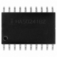
HA5024IBZ Intersil, HA5024IBZ Datasheet - Page 7

HA5024IBZ
Manufacturer Part Number
HA5024IBZ
Description
IC OPAMP QUAD 125MHZ 20-SOIC
Manufacturer
Intersil
Datasheet
1.HA5024IBZ.pdf
(16 pages)
Specifications of HA5024IBZ
Applications
Current Feedback
Number Of Circuits
4
-3db Bandwidth
125MHz
Slew Rate
350 V/µs
Current - Supply
7.5mA
Current - Output / Channel
20mA
Voltage - Supply, Single/dual (±)
±4.5 V ~ 18 V
Mounting Type
Surface Mount
Package / Case
20-SOIC (0.300", 7.50mm Width)
Peak Reflow Compatible (260 C)
Yes
Rohs Compliant
Yes
Lead Free Status / RoHS Status
Lead free / RoHS Compliant
Available stocks
Company
Part Number
Manufacturer
Quantity
Price
Part Number:
HA5024IBZ
Manufacturer:
INFTEL
Quantity:
20 000
Application Information
Optimum Feedback Resistor
The plots of inverting and non-inverting frequency response,
see Figure 11 and Figure 12 in the Typical Performance
Curves section, illustrate the performance of the HA5024 in
various closed loop gain configurations. Although the
bandwidth dependency on closed loop gain isn’t as severe
as that of a voltage feedback amplifier, there can be an
appreciable decrease in bandwidth at higher gains. This
decrease may be minimized by taking advantage of the
current feedback amplifier’s unique relationship between
bandwidth and R
feedback resistor, even for unity gain applications, and R
in conjunction with the internal compensation capacitor, sets
the dominant pole of the frequency response. Thus, the
amplifier’s bandwidth is inversely proportional to R
HA5024 design is optimized for a 1000Ω R
Decreasing R
resulting in excessive peaking and overshoot. At higher
gains the amplifier is more stable, so R
in a trade-off of stability for bandwidth.
The table below lists recommended R
gains, and the expected bandwidth.
PC Board Layout
The frequency response of this amplifier depends greatly on
the amount of care taken in designing the PC board. The
use of low inductance components such as chip resistors
and chip capacitors is strongly recommended. If leaded
components are used the leads must be kept short
especially for the power supply decoupling components and
those components connected to the inverting input.
Attention must be given to decoupling the power supplies. A
large value (10µF) tantalum or electrolytic capacitor in
parallel with a small value (0.1µF) chip capacitor works well
in most cases.
A ground plane is strongly recommended to control noise.
Care must also be taken to minimize the capacitance to
ground seen by the amplifier’s inverting input (-IN). The
larger this capacitance, the worse the gain peaking, resulting
in pulse overshoot and possible instability. It is
recommended that the ground plane be removed under
traces connected to -IN, and that connections to -IN be kept
as short as possible to minimize the capacitance from this
node to ground.
GAIN (A
+10
-10
+1
+2
+5
-1
CL
)
F
in a unity gain application decreases stability,
F
. All current feedback amplifiers require a
R
1000
1000
750
681
383
750
F
(Ω)
7
F
F
BANDWIDTH (MHz)
values for various
can be decreased
F
at a gain of +1.
100
125
95
52
65
22
F
. The
F
,
HA5024
Driving Capacitive Loads
Capacitive loads will degrade the amplifier’s phase margin
resulting in frequency response peaking and possible
oscillations. In most cases the oscillation can be avoided by
placing an isolation resistor (R) in series with the output as
shown in Figure 6.
The selection criteria for the isolation resister is highly
dependent on the load, but 27Ω has been determined to be
a good starting value.
Power Dissipation Considerations
Due to the high supply current inherent in quad amplifiers, care
must be taken to insure that the maximum junction temperature
(T
shows the maximum ambient temperature versus supply
voltage for the available package styles (Plastic DIP, SOIC). At
±5V
operated over the full industrial range of -40°C to 85°C. It is
recommended that thermal calculations, which take into
account output power, be performed by the designer.
Enable/Disable Function
When enabled the amplifier functions as a normal current
feedback amplifier with all of the data in the electrical
specifications table being valid and applicable. When
disabled the amplifier output assumes a true high
impedance state and the supply current is reduced
significantly.
J,
FIGURE 6. PLACEMENT OF THE OUTPUT ISOLATION
FIGURE 7. MAXIMUM OPERATING AMBIENT TEMPERA-
DC
see Absolute Maximum Ratings) is not exceeded. Figure 7
130
120
110
100
90
80
70
60
50
quiescent operation both package styles may be
V
IN
5
RESISTOR, R
TURE vs SUPPLY VOLTAGE
R
7
100Ω
T
R
I
SUPPLY VOLTAGE (±V)
+
-
9
PDIP
R
F
R
SOIC
11
C
13
L
February 8, 2006
V
OUT
15
3550.6


