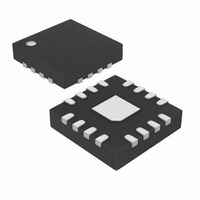
MAX3654ETE+T Maxim Integrated Products, MAX3654ETE+T Datasheet - Page 6

MAX3654ETE+T
Manufacturer Part Number
MAX3654ETE+T
Description
IC AMP TRANSIMPEDANCE 16-TQFN
Manufacturer
Maxim Integrated Products
Type
Transimpedance Amplifierr
Datasheet
1.MAX3654ETE.pdf
(8 pages)
Specifications of MAX3654ETE+T
Applications
CATV
Mounting Type
Surface Mount
Package / Case
16-TQFN Exposed Pad
Lead Free Status / RoHS Status
Lead free / RoHS Compliant
The MAX3654 is a broadband, high-linearity, low-noise
transimpedance amplifier. The transimpedance (gain)
can be adjusted between 43.5dBΩ and 62dBΩ using
the voltage at an external control input (VAGC). When
connected as shown in the Typical Application Circuit,
optical input levels from -6dBm to +2dBm will produce
a minimum output of 14dBmV/channel, and 4dB tilt
compensation. Gain deviation over frequency from
47MHz to 870MHz is less than ±0.75dB.
The input stage is a low-noise analog transimpedance
amplifier (TIA) connected differentially to the analog
photodiode. Desired performance can be achieved
with a photodiode having capacitance (C
The gain-control pin VAGC sets overall TIA gain imple-
mented as three switchable gain stages, each with a
continuously variable gain control, as shown in Figure 3.
This produces a continuously variable gain ranging
from 62dBΩ (at VAGC = 0.175V) to 43.5dBΩ at
(VAGC=1.4V). A set of comparators examines the
47MHz to 870MHz Analog CATV
Transimpedance Amplifier
6
1, 4, 9, 12
8, 14, 16
_______________________________________________________________________________________
PIN
EP
10
11
13
15
2
3
5
6
7
Low-Noise Variable Gain Amplifier
NAME
TEST1
TEST2
VAGC
MUTE
OUT+
HYST
OUT-
VAGC and Hysteresis Control
GND
V
IN+
IN-
EP
CC
Detailed Description
+5.0V Power Supply
Positive Analog Photodiode Input Connection. Typically connected to photodiode cathode.
Negative Analog Photodiode Input Connection. Typically connected to photodiode anode.
AGC Control Input. Range is 0 to 1.4V. See the Typical Operating Characteristics Gain vs. Control
Voltage graph.
Mute Control Input, TTL. MUTE < 0.8V to mute output.
AGC Hysteresis Control Input. A resistor from HYST to GND controls the hysteresis level.
Ground
Negative RF Output. The voltage on this pin decreases with increasing optical power when IN+ is
connected to the photodiode cathode.
Positive RF Output. The voltage on this pin increases with increasing optical power when IN- is
connected to the photodiode anode.
Reserved for Test. Connect to GND for normal operation.
Reserved for Test. Connect to GND for normal operation.
Exposed Pad. The exposed pad must be soldered to the circuit-board ground for proper thermal and
electrical performance.
PD
) up to 1pF.
VAGC input to select a gain stage. As the voltage at
VAGC crosses the two locations in the gain vs. VAGC
curve, where the gain stage changes (350mV and
700mV), there will be small deviations in the output
which may lead to a brief interruption of CATV signals.
See the Typical Operating Characteristics for Gain vs.
Control Voltage.
A hysteresis control input is provided to limit dithering
when the optical level is close to a gain-switching point.
The hysteresis level is controlled by the value of R
Hysteresis is minimum (0.13dB) when this pin is open.
With a typical photodiode, the gain at 870MHz is 4dB
higher than at 47MHz. The overall frequency response
of the TIA is within ±0.75dB of a straight line connecting
the values at 47MHz and 870MHz.
In normal operation, the TTL MUTE pin is held high.
When MUTE is low, the output signal is attenuated by
more than 45dB.
RF Output and Cable Tilt Compensation
FUNCTION
Pin Description
Mute
HYST
.


