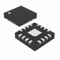
MAX3654ETE+T Maxim Integrated Products, MAX3654ETE+T Datasheet - Page 2

MAX3654ETE+T
Manufacturer Part Number
MAX3654ETE+T
Description
IC AMP TRANSIMPEDANCE 16-TQFN
Manufacturer
Maxim Integrated Products
Type
Transimpedance Amplifierr
Datasheet
1.MAX3654ETE.pdf
(8 pages)
Specifications of MAX3654ETE+T
Applications
CATV
Mounting Type
Surface Mount
Package / Case
16-TQFN Exposed Pad
Lead Free Status / RoHS Status
Lead free / RoHS Compliant
ABSOLUTE MAXIMUM RATINGS
Supply Voltage, VCC.............................................-0.3V to +6.0V
IN+, IN-, VAGC, OUT+, OUT-,
TEST1, TEST2........................................................-0.3V to +5.5V
Output Current (OUT+, OUT-) ............................................56mA
AC ELECTRICAL CHARACTERISTICS
(V
47MHz to 870MHz Analog CATV
Transimpedance Amplifier
DC ELECTRICAL CHARACTERISTICS
(V
Stresses beyond those listed under “Absolute Maximum Ratings” may cause permanent damage to the device. These are stress ratings only, and functional
operation of the device at these or any other conditions beyond those indicated in the operational sections of the specifications is not implied. Exposure to
absolute maximum rating conditions for extended periods may affect device reliability.
Note 1: DC parameters are tested at +25°C, and guaranteed by design and characterization at -40°C and +85°C.
Note 2: Maximum difference between frequency response at any point and a straight line connecting frequency response at
Note 3: Gain control stability is the maximum variation in transimpedance (over process, voltage, and temperature) for any V
Note 4: AC parameters guaranteed by design and characterization.
Note 5: OIP2 and OIP3 measured using two tones at f1 = 800MHz and f2 = 850MHz, P
Note 6: Includes the effects of a packaged photodiode having the characteristics shown in Figure 2.
2
Supply Current
Gain Control Input Current
Mute Input High
Mute Input Low
Mute Input Current
Operating Frequency Range
Frequency Response Flatness
Transimpedance, Differential (Z
Gain Control Stability
Gain Tilt
Output Second-Order Intercept
Output Third-Order Intercept
Equivalent Input Noise Including
Photodiode
Gain Hysteresis, Optical
Differential Output Level, Mute
RF Output Return Loss
CC
CC
_______________________________________________________________________________________
= +4.75V to +5.25V, output ZL = 75Ω, typical values at V
= +4.75V to +5.25V, typical values at V
end points.
control voltage.
PARAMETER
PARAMETER
MUTE, HYST.........-0.3V to +5.5V
T
)
SYM B O L
SYM B O L
I
OIP2
OIP3
IL
-S22
EIN
I
V
V
CC
, I
f
IH
IL
IH
CC
= +5.0V, T
V
47MHz to 870MHz (Notes 2, 6)
47MHz
V
Linear, 870MHz compared to 47MHz
(Notes 4, 6)
(Note 5)
(Notes 4, 5)
V
R
R
MUTE ≤ 0.8V, 50MHz
47MHz to 870MHz
AGC
AGC
AGC
HYST
HYST
= 0 to 1.4V, R
= 1.4V
≤ 0.175V (Notes 4, 6)
= open
= GND
A
= +25°C, unless otherwise noted.) (Note 1)
CC
CONDITIONS
CONDITIONS
= +5.0V, T
V
V
V
Continuous Power Dissipation, 16-Lead TQFN-EP Package
Operating Temperature Range ...........................-40°C to +85°C
Storage Temperature Range .............................-55°C to +150°C
Lead Temperature (soldering,10s) ..................................+300°C
HYST
AGC
AGC
AGC
(T
A
= open (Note 3)
≤ 0.175V
= 0.500V
= 1.400V
A
= +70°C) (derate 16.9mW/°C above +70°C)....1349.1mW
= +25°C, unless otherwise noted.)
OUT
= -16dBm, V
60.5
51.5
MIN
MIN
2.0
47
42
18
3
AGC
±0.75
±0.13
±0.65
±0.3
TYP
TYP
43.5
136
>47
-58
50
62
53
21
13
4
= 1.4V.
±0.75
MAX
MAX
±1.6
63.5
54.5
170
200
870
-45
0.8
5.5
30
45
8
pA/√Hz
UNITS
UNITS
MHz
dBΩ
dBm
dBm
dBc
mA
dB
dB
dB
dB
dB
µA
µA
V
V
AGC


