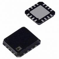
ADA4938-1ACPZ-R2 Analog Devices Inc, ADA4938-1ACPZ-R2 Datasheet - Page 20

ADA4938-1ACPZ-R2
Manufacturer Part Number
ADA4938-1ACPZ-R2
Description
IC ADC DRIVER DIFF 16-LFCSP
Manufacturer
Analog Devices Inc
Type
ADC Driverr
Datasheet
1.ADA4938-1ACPZ-R7.pdf
(28 pages)
Specifications of ADA4938-1ACPZ-R2
Applications
Data Acquisition
Mounting Type
Surface Mount
Package / Case
16-LFCSP
No. Of Amplifiers
1
Input Offset Voltage
4mV
Gain Db Max
1.05dB
Bandwidth
1GHz
Slew Rate
4700V/µs
Supply Voltage Range
4.5V To 11V
Supply Current
37mA
Amplifier Case Style
LFCSP
Rohs Compliant
Yes
Lead Free Status / RoHS Status
Lead free / RoHS Compliant
ADA4938-1/ADA4938-2
Similar to the case of a conventional op amp, the output noise
voltage densities can be estimated by multiplying the input-
referred terms at +IN and −IN by the appropriate output factor,
where:
When R
becomes
Note that the output noise from V
The total differential output noise density, v
square of the individual output noise terms.
THE IMPACT OF MISMATCHES IN THE FEEDBACK
NETWORKS
As previously mentioned, even if the external feedback networks
(R
loop still forces the outputs to remain balanced. The amplitudes
of the signals at each output remain equal and 180° out of phase.
The input-to-output, differential mode gain varies proportionately
to the feedback mismatch, but the output balance is unaffected.
As well as causing a noise contribution from V
errors in the external resistors result in a degradation of the
ability of the circuit to reject input common-mode signals, much
the same as for a four-resistor difference amplifier made from a
conventional op amp.
In addition, if the dc levels of the input and output common-
mode voltages are different, matching errors result in a small
differential-mode output offset voltage. When G = +1, with a
ground referenced input signal and the output common-mode
level set to 2.5 V, an output offset of as much as 25 mV (1% of
the difference in common-mode levels) can result if 1% tolerance
resistors are used. Resistors of 1% tolerance result in a worst-case
input CMRR of about 40 dB, a worst-case differential-mode
output offset of 25 mV due to 2.5 V level-shift, and no significant
degradation in output balance error.
G
β
1
N
F
=
/R
=
G
v
R
G
(
nOD
) are mismatched, the internal common-mode feedback
F1
N
β
R
1
F1
=
+
G1
+
2
/R
=
R
1
β
β
G1
G1
2
=
i
)
∑
= R
=
8
1
is the circuit noise gain.
and
1
+
v
nOi
2
F2
R
R
/R
G
F
β
2
G2
=
, β1 = β2 = β, and the noise gain
R
F2
R
+
G2
R
G2
OCM
are the feedback factors.
goes to zero in this case.
nOD
OCM
, is the root-sum-
, ratio matching
Rev. A | Page 20 of 28
CALCULATING THE INPUT IMPEDANCE OF AN
APPLICATION CIRCUIT
The effective input impedance of a circuit depends on whether
the amplifier is being driven by a single-ended or differential
signal source. For balanced differential input signals, as shown
in Figure 59, the input impedance (R
(+D
For an unbalanced, single-ended input signal (see Figure 60),
the input impedance is
The input impedance of the circuit is effectively higher than it
would be for a conventional op amp connected as an inverter
because a fraction of the differential output voltage appears at
the inputs as a common-mode signal, partially bootstrapping
the voltage across the Input Gain Resistor R
INPUT COMMON-MODE VOLTAGE RANGE IN
SINGLE-SUPPLY APPLICATIONS
The ADA4938 is optimized for level-shifting, ground-referenced
input signals. As such, the center of the input common-mode
range is shifted approximately 1 V down from midsupply. The
input common-mode range at the summing nodes of the amplifier
is from 0.3 V above −V
the outputs, the voltage swing at the +IN and −IN terminals must
be confined to these ranges.
Figure 60. ADA4938-x Configured for Unbalanced (Single-Ended) Input
IN
Figure 59. ADA4938 Configured for Balanced (Differential) Inputs
and −D
R
+D
–D
S
IN
IN
IN
) is simply R
R
R
T
S
R
R
G
G
R
IN
S
R
V
,
R
to 1.6 V below +V
cm
G
R
OCM
T
+IN
–IN
G
=
V
IN, dm
ADA4938
OCM
⎛
⎜
⎜
⎜
⎜
⎝
1
+V
R
R
−
= 2 × R
F
S
F
ADA4938
R
R
2
F
F
×
+V
IN, dm
R
(
R
S
G
R
G
G
F
) between the inputs
.
+
S
R
V
. To avoid clipping at
G
OUT, dm
F
.
)
⎞
⎟
⎟
⎟
⎟
⎠
V
OUT, dm


