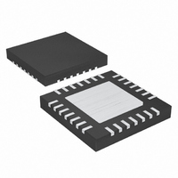
MAX9730ETI+T Maxim Integrated Products, MAX9730ETI+T Datasheet - Page 9

MAX9730ETI+T
Manufacturer Part Number
MAX9730ETI+T
Description
IC AMP AUDIO PWR 2.4W G 28TQFN
Manufacturer
Maxim Integrated Products
Type
Class Gr
Datasheet
1.MAX9730ETI.pdf
(12 pages)
Specifications of MAX9730ETI+T
Output Type
1-Channel (Mono)
Max Output Power X Channels @ Load
2.4W x 1 @ 8 Ohm
Voltage - Supply
2.7 V ~ 5.5 V
Features
Depop, Differential Inputs, Shutdown
Mounting Type
Surface Mount
Package / Case
28-TQFN Exposed Pad
Lead Free Status / RoHS Status
Lead free / RoHS Compliant
In differential input configurations, the common-mode
rejection ratio (CMRR) is primarily limited by the exter-
nal resistor and capacitor matching. Ideally, to achieve
the highest possible CMRR, the following external com-
ponents should be selected where:
and
The AC-coupling capacitors (C
(R
an input signal (see the Typical Application
Circuit/Functional Diagram ). C
from the amplifier. The -3dB point of the highpass filter,
assuming zero source impedance due to the input signal
source, is given by:
Choose C
quency of interest. Setting f
amplifier’s low frequency response. Use capacitors with
low-voltage coefficient dielectrics. Aluminum electrolytic,
tantalum, or film dielectric capacitors are good choices
for AC-coupling capacitors. Capacitors with high-voltage
coefficients, such as ceramics (non-C0G dielectrics),
can result in increased distortion at low frequencies.
Use capacitors with an ESR less than 50mΩ for opti-
mum performance. Low-ESR ceramic capacitors mini-
mize the output resistance of the charge pump. For
best performance over the extended temperature
range, select capacitors with an X7R dielectric.
The value of the flying capacitor (C1) affects the load
regulation and output resistance of the charge pump. A
C1 value that is too small degrades the device’s ability
IN_
) form highpass filters that remove any DC bias from
2.4W, Single-Supply, Class G Power Amplifier
IN
so that f
f
−
3
dB
_______________________________________________________________________________________
=
Charge-Pump Capacitor Selection
R
2π
R
-3dB
C
FB
IN
IN
×
+
+
+
R
is well below the lowest fre-
=
IN
=
Component Selection
Input-Coupling Capacitor
1
C
R
_
R
-3dB
FB
IN
IN
×
IN_
IN_
C
−
−
−
Flying Capacitor (C1)
IN
) and input resistors
too high affects the
blocks DC voltages
_
( )
Hz
to provide sufficient current drive. Increasing the value
of C1 improves load regulation and reduces the charge-
pump output resistance to an extent. Above 1µF, the on-
resistance of the switches and the ESR of C1 and C2
dominate. A 4.7µF capacitor is recommended.
The output capacitor value and ESR directly affect the
ripple at PV
Likewise, decreasing the ESR of C2 reduces both rip-
ple and output resistance. A 10µF capacitor is recom-
mended.
The charge pump operates in two modes. When the
charge pump is loaded below 100mA, it operates in a
slow mode where the oscillation frequency is reduced
to 1/4 of its normal operating frequency. Once loaded,
the charge-pump oscillation frequency returns to nor-
mal operation. In applications where the design may be
sensitive to the operating charge-pump oscillation fre-
quency, the value of the external resistor R
changed to adjust the charge-pump oscillation fre-
quency (see Figure 4).
Figure 4. Charge-Pump Oscillation Frequency vs. R
Charge-Pump Frequency Set Resistor (R
600
550
500
450
400
350
300
250
200
SS
50
. Increasing C2 reduces output ripple.
CHARGE-PUMP OSCILLATION
75
FREQUENCY vs. R
R
FS
100
(kΩ)
I
Hold Capacitor (C2)
LOAD
FS
125
> 100mA
150
FS
FS
can be
FS
9
)


