LM4927SD/NOPB National Semiconductor, LM4927SD/NOPB Datasheet - Page 4
LM4927SD/NOPB
Manufacturer Part Number
LM4927SD/NOPB
Description
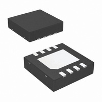
IC AMP AUDIO PWR 2.5W MONO 8LLP
Manufacturer
National Semiconductor
Series
Boomer®r
Type
Class ABr
Datasheet
1.LM4927SDNOPB.pdf
(14 pages)
Specifications of LM4927SD/NOPB
Output Type
1-Channel (Mono)
Max Output Power X Channels @ Load
2.5W x 1 @ 4 Ohm
Voltage - Supply
2.4 V ~ 5.5 V
Features
Depop, Differential Inputs, Shutdown, Thermal Protection
Mounting Type
Surface Mount
Package / Case
8-LLP
For Use With
LM4927SDBD - BOARD EVALUATION LM4927SD
Lead Free Status / RoHS Status
Lead free / RoHS Compliant
Other names
LM4927SD
LM4927SDNOPB
LM4927SDNOPBTR
LM4927SDNOPBTR
LM4927SDTR
LM4927SDNOPB
LM4927SDNOPBTR
LM4927SDNOPBTR
LM4927SDTR
Available stocks
Company
Part Number
Manufacturer
Quantity
Price
Company:

Part Number:
LM4927SD/NOPB
Manufacturer:
NS
Quantity:
9 435


www.national.com
P
THD+N
PSRR
CMRR
V
V
V
T
Symbol
WU
o
OS
SDIH
SDIL
Electrical Characteristics V
The following specifications apply for V
25˚C. (Continued)
Note 1: All voltages are measured with respect to the ground pin, unless otherwise specified.
Note 2: Absolute Maximum Ratings indicate limits beyond which damage to the device may occur. Operating Ratings indicate conditions for which the device is
functional, but do not guarantee specific performance limits. Electrical Characteristics state DC and AC electrical specifications under particular test conditions which
guarantee specific performance limits. This assumes that the device is within the Operating Ratings. Specifications are not guaranteed for parameters where no limit
is given, however, the typical value is a good indication of device performance.
Note 3: The maximum power dissipation must be derated at elevated temperatures and is dictated by T
allowable power dissipation is P
derating curve for additional information.
Note 4: Human body model, 100pF discharged through a 1.5kΩ resistor.
Note 5: Machine Model, 220pF – 240pF discharged through all pins.
Note 6: Typicals are measured at 25˚C and represent the parametric norm.
Note 7: Limits are guaranteed to National’s AOQL (Average Outgoing Quality Level).
Note 8: 10Ω terminated input.
Note 9: When driving 4Ω loads from a 5V power supply, the LM4927LD must be mounted to a circuit board with the exposed-DAP area soldered down to a 1in
plane of 1oz, copper.
Note 10: Data taken with BW = 80kHz and A
External Components Description
Components
(Figure 1)
1.
2.
3.
4.
Output Power
Total Harmonic Distortion+Noise
Power Supply Rejection Ratio
Common-Mode Rejection Ratio
Output Offset
Shutdown Voltage Input High
Shutdown Voltage Input Low
Wake-up time from Shutdown
C
C
R
R
S
B
i
f
Supply bypass capacitor which provides power supply filtering. Refer to the Power Supply Bypassing
section for information concerning proper placement and selection of the supply bypass capacitor.
Bypass pin capacitor which provides half-supply filtering. Refer to the section, Proper Selection of External
Components, for information concerning proper placement and selection of C
Inverting input resistance which sets the closed-loop gain in conjunction with R
Internal feedback resistance which sets the closed-loop gain in conjunction with R
Parameter
DMAX
= (T
JMAX
V
= 1/1 except where specified.
– T
DD
A
) / θ
= 3V, A
JA
DD
THD = 1% (max); f = 1 kHz
THD = 10% (max); f = 1 kHz
P
V
f = 217Hz, V
V
Cbypass
or the number given in Absolute Maximum Ratings, whichever is lower. For the LM4927, see power
o
ripple
IN
V
R
R
R
R
= 3V
= 0.25Wrms; f = 1kHz
= 0V
f = 217Hz (Note 8)
f = 1kHz (Note 8)
L
L
L
L
= 1, and 8Ω load unless otherwise specified. Limits apply for T
= 4Ω
= 8Ω
= 4Ω
= 8Ω
= 200mV sine p-p
(Notes 1, 2)
Conditions
CM
Functional Description
4
= 200mV
pp
JMAX
, θ
JA
(Note 6)
Typical
0.650
0.450
0.800
0.550
, and the ambient temperature T
0.04
85
80
60
4
8
LM4927
B
f
.
.
i
.
(Note 7)
Limit
1.4
0.4
A
. The maximum
A
=
mV (max)
(Limits)
V (max)
V (min)
Units
ms
dB
dB
W
W
%
2
Related parts for LM4927SD/NOPB
Image
Part Number
Description
Manufacturer
Datasheet
Request
R

Part Number:
Description:
IC,Audio Amplifier,SINGLE,LLCC,8PIN,PLASTIC
Manufacturer:
National Semiconductor
Part Number:
Description:
National Semiconductor [8-Bit D/A Converter]
Manufacturer:
National Semiconductor
Datasheet:
Part Number:
Description:
National Semiconductor [Media Coprocessor]
Manufacturer:
National Semiconductor
Datasheet:
Part Number:
Description:
Digitally Controlled Tone and Volume Circuit with Stereo Audio Power Amplifier, Microphone Preamp Stage and National 3D Sound
Manufacturer:
National Semiconductor
Datasheet:
Part Number:
Description:
Digitally Controlled Tone and Volume Circuit with Stereo Audio Power Amplifier, Microphone Preamp Stage and National 3D Sound
Manufacturer:
National Semiconductor
Datasheet:
Part Number:
Description:
AC97 Rev 2 Codec with Sample Rate Conversion and National 3D Sound
Manufacturer:
National Semiconductor
Part Number:
Description:
Manufacturer:
National Semiconductor
Datasheet:
Part Number:
Description:
Manufacturer:
National Semiconductor
Datasheet:
Part Number:
Description:
General Purpose, Low Voltage, Low Power, Rail-to-Rail Output Operational Amplifiers
Manufacturer:
National Semiconductor
Datasheet:
Part Number:
Description:
8-bit 20 MSPS flash A/D converter.
Manufacturer:
National Semiconductor
Datasheet:
Part Number:
Description:
Low Noise Quad Operational Amplifier
Manufacturer:
National Semiconductor
Datasheet:
Part Number:
Description:
Quad Differential Line Receivers
Manufacturer:
National Semiconductor
Datasheet:
Part Number:
Description:
Quad High Speed Trapezoidal? Bus Transceiver
Manufacturer:
National Semiconductor
Datasheet:
Part Number:
Description:
Dual Line Receiver
Manufacturer:
National Semiconductor
Datasheet: