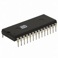
ISD5116PY Nuvoton Technology Corporation of America, ISD5116PY Datasheet - Page 24

ISD5116PY
Manufacturer Part Number
ISD5116PY
Description
IC VOICE REC/PLAY 8-16MN 28-DIP
Manufacturer
Nuvoton Technology Corporation of America
Series
ISD5100r
Datasheet
1.ISD5116SY.pdf
(90 pages)
Specifications of ISD5116PY
Interface
I²C
Filter Pass Band
1.7 ~ 3.4kHz
Duration
8 ~ 16 Min
Mounting Type
Through Hole
Package / Case
28-DIP (0.600", 15.24mm)
For Use With
ISD-ES511 - EVALUATION SYSTEM FOR ISD5100ISD-ES501 - EVALUATION SYSTEM FOR ISD5008
Lead Free Status / RoHS Status
Lead free / RoHS Compliant
Available stocks
Company
Part Number
Manufacturer
Quantity
Price
Company:
Part Number:
ISD5116PY
Manufacturer:
Intersil
Quantity:
360
The end result of the above set up is
CFG0=0100 0100 0000 1011 (hex 440B)
and
CFG1=0000 0001 1110 0011 (hex 01E3).
Since both registers are being loaded, CFG0 is loaded, followed by the loading of CFG1. These two
registers must be loaded in this order. The internal set up for both registers will take effect synchro-
nously with the rising edge of SCL.
The call record mode adds the ability to record an incoming phone call. In most applications, the
ISD5100 Series would first be set up for Feed Through Mode as described above. When the user
wishes to record the incoming call, the setup of the chip is modified to add that ability. For the purpose
of this explanation, we will use the 6.4 kHz sample rate during recording.
The block diagram of the ISD5100 Series shows that the Multilevel Storage array is always driven
from the SUM2 SUMMING amplifier. The path traces back from there through the LOW PASS Filter,
THE FILTER MUX, THE SUM1 SUMMING amplifier, the SUM1 MUX, then from the ANA in amplifier.
Feed Through Mode has already powered up the ANA IN amp so we only need to power up and
enable the path to the Multilevel Storage array from that point:
6. Don’t Care bits — The following stages are not used in Feed Through Mode. Their bits may be
1. Select the ANA IN path through the SUM1 MUX—Bits S1S0 and S1S1 control the state of the
2. Select the SUM1 MUX input (only) to the S1 SUMMING amplifier—Bits S1M0 and S1M1
set to either level. In this example, we will set all the following bits to a ZERO. (a). Bit INS0, bit
D9 of CFG0 controls the Input Source Mux. (b). Bits AXG0 and AXG1 are bits D11 and D12
respectively in CFG0. They control the AUX IN amplifier gain setting. (c). Bits FLD0 and FLD1
are bits D2 and D3 respectively in CFG1. They control the sample rate and filter band pass
setting. (d). Bit FLS0 is bit D4 in CFG1. It controls the FILTER MUX. (e). Bits S1S0 and S1S1
are bits D9 and D10 of CFG1. They control the SUM1 MUX. (f). Bits VOL0, VOL1 and VOL2
are bits D11, D12 and D13 of CFG1. They control the setting of the Volume Control. (g). Bits
VLS0 and VLS1 are bits D14 and D15 of CFG1. They control the Volume Control MUX.
6.3.8
SUM1 MUX. These are bits D9 and D10 respectively of CFG1 and they should be set to the
state where both D9 and D10 are ZERO to select the ANA IN path.
control the state of the SUM1 SUMMING amplifier. These are bits D7 and D8 respectively of
CFG1 and they should be set to the state where D7 is ONE and D8 is ZERO to select the
SUM1 MUX (only) path.
Call Record
- 24 -
Publication Release Date: Oct 31, 2008
ISD5100 SERIES
Revision 1.42


