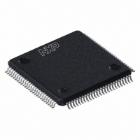
SC28L198A1BE,557 NXP Semiconductors, SC28L198A1BE,557 Datasheet - Page 30

SC28L198A1BE,557
Manufacturer Part Number
SC28L198A1BE,557
Description
IC UART OCTAL W/FIFO 100-LQFP
Manufacturer
NXP Semiconductors
Datasheet
1.SC28L198A1BE557.pdf
(57 pages)
Specifications of SC28L198A1BE,557
Features
False-start Bit Detection
Number Of Channels
8
Fifo's
16 Byte
Voltage - Supply
3.3V, 5V
With Auto Flow Control
Yes
With False Start Bit Detection
Yes
With Modem Control
Yes
With Cmos
Yes
Mounting Type
Surface Mount
Package / Case
100-LQFP
Lead Free Status / RoHS Status
Lead free / RoHS Compliant
Other names
568-1210
935262731557
SC28L198A1BE
935262731557
SC28L198A1BE
Available stocks
Company
Part Number
Manufacturer
Quantity
Price
Company:
Part Number:
SC28L198A1BE,557
Manufacturer:
NXP Semiconductors
Quantity:
10 000
Philips Semiconductors
Table 38. I/OPCR – I/O Port Configuration Register
* If I/OPCR(5:4) is programmed as ’01’ then the RTSN functionality
is assigned to I/O2, otherwise, this function can be implemented on
I/O1. (This allows for a lower pin count package option)
This register contains 4, 2 bit fields that set the direction and source
for each of the I/O pins associated with the channel. The I/O2
output may be RTSN if MR1[7] is set, or may signal ”end of
transmission” if MR2[5] is set.(Please see the descriptions of these
functions under the MR1 and MR2 register descriptions) If this
control bit is cleared, the pin will use the OPR[2] as a source if
I/OPCR[5:4] is b’01. The b’00 combinations are always inputs. This
register resets to x’0, effectively configuring all I/O pins as inputs on
power up or reset. Inputs may be used as RxC, TxC inputs or
CTSN and General Purpose Inputs simultaneously. All inputs are
equipped with change detectors that may be used to generate
interrupts or can be polled, as required.
NOTE: To ensure that CTSN, RTSN and an external RxC are
always available, if I/O2 is not selected as the RTSN output, the
RTSN function is automatically provided on I/O1.
GENERAL PURPOSE OUTPUT PIN CONTROL
The following four registers control the function of the G
These output pins have a unique control matrix which includes a
clocking mechanism that will allow the pin to change synchronously
with an internal or external stimulus. See diagram below.
Table 39. GPOSR – General Purpose Output
GPOSR selects the signal or data source for the G
and Rx clock selection is straight forward. The selection of the
GPOR allows a more flexible timing control of when the G
changes.
2006 Aug 10
Bits 7:6
I/O3 control
00 – GPI/TxC input
01 – I/OPIOR[3] output
10 – TxC16x output
11 – TxC1x output
Bits 7:4
Reserved
Octal UART for 3.3 V and 5 V supply voltage
Select Register
Bits 3:0
Global General Purpose Output 0 Selection
0000 – 0111 reserved
1000 = TxC1x a
1001 = TxC16x a
1010 = RxC16x a
1011 = TxC16x b
1100 = GGPOR(3)
1101 = GGPOR(2)
1110 = GGPOR(1)
1111 = GGPOR(0)
Bits 5:4
I/O2 control
00 – GPI/RxC input
01 – I/OPIOR[2]/RTSN *
10 – RxC1x output
11 – RxC16x output
OUT
0 pin. The Tx
OUT
OUT
0 pin.
0 pin
30
Bits 3:2
I/O1 control
00 – GPI input
01 – I/OPIOR[1]/RTSN *
10 – Reserved
11 – RxC1x output
Table 40. GPOR – General Purpose Output
This register is a read/write register. Its contents may be altered by
a GPOR Write or by the GPOC and GPOD registers shown below.
The GPOD and GPOC may be programmed to cause the individual
bits of the GPOR to change synchronously with internal or external
events. The cells of this register may be thought of as a “Two Port
flip-flop”; one port is controlled by a D input and clock, the other by a
data load strobe. A read of the GPOR always returns its current
value regardless of the port from which it was loaded.
Table 41. GPOC – General Purpose Output Clk
This controls the clock source for GPOR that will clock and/or toggle
the data from the selected GPOD source. When code b’00 is
selected, no clock will be provided, thereby preventing any change
through the D port.
Table 42. GPOD – General Purpose Output Data
This register selects the data that will be presented to the GPOR “D”
input. Note that selection b’10 selects the inverted GPOR data as
the input. In this case, the GPOR output will toggle synchronously
with the clock selected in the GPOC.
Bits 7:4
Reserved
Bits 7:6
Clk Sel
GPOR(3)
00 = none
01 = G
10 = G
11 = reserved
Bits 7:6
Data Sel
GPOR(3)
00 = ’1’
01 = ’0’
10 = GPOR3N
11 = reserved
IN
IN
0
1
Register
Register
Register
Bit 3
GPOR(3)
Bits 5:4
Clk Sel
GPOR(2)
00 = none
01 = G
10 = G
11 = reserved
Bits 5:4
Data Sel
GPOR(2)
00 = ’1’
01 = ’0’
10 = GPOR2N
11 = reserved
IN
IN
0
1
Bit 2
GPOR(2)
Bits 1:0
I/O0 control
00 – GPI/CTSN input
01 – I/OPIOR[0]output
10 – TxC1x output
11 – TxC16x output
Bits 3:2
Clk Sel
GPOR(1)
00 = none
01 = G
10 = G
11 = I/O3c
Bits 3:2
Data Sel
GPOR(1)
00 = ’1’
01 = ’0’
10 = GPOR1N
11 = I/O3d
Bit 1
GPOR(1)
IN
IN
0
1
SC28L198
Product data sheet
Bits 1:0
Clk Sel
GPOR(0)
00 = none
01 = G
10 = G
11 = I/O3a
Bits 1:0
Data Sel
GPOR(0)
00 = ’1’
01 = ’0’
10 = GPOR0N
11 = I/O3b
GPOR(0)
Bit 0
IN
IN
0
1


