SC28L194A1BE,557 NXP Semiconductors, SC28L194A1BE,557 Datasheet - Page 5
SC28L194A1BE,557
Manufacturer Part Number
SC28L194A1BE,557
Description
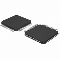
IC UART QUAD W/FIFO 80-LQFP
Manufacturer
NXP Semiconductors
Datasheet
1.SC28L194A1BE528.pdf
(52 pages)
Specifications of SC28L194A1BE,557
Features
False-start Bit Detection
Number Of Channels
4, QUART
Fifo's
16 Byte
Voltage - Supply
3.3V, 5V
With Auto Flow Control
Yes
With False Start Bit Detection
Yes
With Modem Control
Yes
With Cmos
Yes
Mounting Type
Surface Mount
Package / Case
80-LQFP
Lead Free Status / RoHS Status
Lead free / RoHS Compliant
Other names
568-1209
935262730557
SC28L194A1BE
935262730557
SC28L194A1BE
Available stocks
Company
Part Number
Manufacturer
Quantity
Price
Company:

Part Number:
SC28L194A1BE,557
Manufacturer:
NXP Semiconductors
Quantity:
10 000


Philips Semiconductors
BLOCK DIAGRAM
As shown in the block diagram, the Quad UART consists of an
interrupt arbiter, host interface, timing blocks and four UART channel
blocks. The four channels blocks operate independently, interacting
only with the timing, host I/F and interrupt blocks.
FUNCTIONAL DESCRIPTION
The SC28L194 is composed of several functional blocks:
CONCEPTUAL OVERVIEW
Host Interface
The Host interface is comprised of the signal pins CEN, W/RN,
IACKN, DACKN, IRQN Sclk and provides all the control for data
transfer between the external and internal data buses of the host
and the QUART. The host interface operates in a synchronous mode
with the system (Sclk) which has been designed for a nominal
operating frequency of 33 MHz. The interface operates in either of
two modes; synchronous or asynchronous to the Sclk However
the bus cycle within the QUART always takes place in four Sclk
cycles after CEN is recognized. These four cycles are the C1, C2,
C3, C4 periods shown in the timing diagrams. DACKN always
occurs in the C4 time and occurs approximately 18 ns after the
rising edge of C4.
Addressing of the various functions of the QUART is through the
address bus A(7:0). To maintain upward compatibility with the
SC28L/C198 Octart the 8 bit address is still defined as such.
However A(6) is NOT used and is internally connected to Vss
(ground). The pin is, therefore, not included in the pin diagram. The
address space is controlled by A(5:0) and A(7). A[7], in a general
sense, is used to separate the data portion of the circuit from the
control portion.
2006 Aug 15
Synchronous host interface block
A timing block consisting of a common baud rate generator
making 22 industry standard baud rates and 2 16-bit counters
used for non-standard baud rate generation
4 identical independent full duplex UART channel blocks
Interrupt arbitration system evaluating 24 contenders
I/O port control section and change of state detectors.
Quad UART for 3.3 V and 5 V supply voltage
INPUT BUFFERS AND OUTPUT DRIVERS
Figure 2. Block Diagram
Block Diagram SC28L194
5
FULL DUPLEX UART CHANNEL
FULL DUPLEX UART CHANNEL
FULL DUPLEX UART CHANNEL
FULL DUPLEX UART CHANNEL
Asynchronous bus cycle
The asynchronous mode requires one bus cycle of the chip select
(CEN) for each read or write to the chip. No more action will occur
on the bus after the C4 time until CEN is returned high.
Synchronous bus cycle
In the synchronous mode a read or write will be done every four
cycles of the Sclk. CEN does not require cycling but must remain
low to keep the synchronous accesses active. This provides a burst
mode of access to the chip.
In both cases each read or write operation(s) will be completed in
four (4) Sclk cycles. The difference in the two modes is only that the
asynchronous mode will not begin another bus cycle if the CEN
remains active after the four internal Sclk have completed. Internally
the asynchronous cycle will terminate after the four periods of Sclk
regardless of how long CEN is held active
In all cases the internal action will terminate at the withdrawal of
CEN. Synchronous CEN cycles shorter than multiples of four Sclk
cycles minus 1 Sclk and asynchronous CEN cycles shorter than four
Sclk cycles may cause short read or write cycles and produce
corrupted data transfers.
Timing Circuits
The timing block consists of a crystal oscillator, a fixed baud rate
generator (BRG), a pair of programmable 16 bit register based
counters. A buffer for the System Clock generates internal timing for
processes not directly concerned with serial data flow.
Crystal Oscillator
The crystal oscillator operates directly from a crystal, tuned between
1.0 and 8.0 MHz, connected across the X1/CCLK and X2 inputs with
a minimum of external components. BRG values listed for the clock
select registers correspond to a 3.6864 MHz crystal frequency. Use
of a 7.3728 MHz crystal will double the Communication Clock
frequencies.
An external clock in the 100 KHz to 10 MHz frequency range may
be connected to X1/CCLK. If an external clock is used instead of a
crystal, X1/CCLK must be driven and X2 left floating. The X1 clock
serves as the basic timing reference for the baud rate generator
(BRG) and is available to the BRG timers. The X1 oscillator input
SD00524
SC28L194
Product data sheet
Related parts for SC28L194A1BE,557
Image
Part Number
Description
Manufacturer
Datasheet
Request
R

Part Number:
Description:
NXP Semiconductors designed the LPC2420/2460 microcontroller around a 16-bit/32-bitARM7TDMI-S CPU core with real-time debug interfaces that include both JTAG andembedded trace
Manufacturer:
NXP Semiconductors
Datasheet:

Part Number:
Description:
NXP Semiconductors designed the LPC2458 microcontroller around a 16-bit/32-bitARM7TDMI-S CPU core with real-time debug interfaces that include both JTAG andembedded trace
Manufacturer:
NXP Semiconductors
Datasheet:
Part Number:
Description:
NXP Semiconductors designed the LPC2468 microcontroller around a 16-bit/32-bitARM7TDMI-S CPU core with real-time debug interfaces that include both JTAG andembedded trace
Manufacturer:
NXP Semiconductors
Datasheet:
Part Number:
Description:
NXP Semiconductors designed the LPC2470 microcontroller, powered by theARM7TDMI-S core, to be a highly integrated microcontroller for a wide range ofapplications that require advanced communications and high quality graphic displays
Manufacturer:
NXP Semiconductors
Datasheet:
Part Number:
Description:
NXP Semiconductors designed the LPC2478 microcontroller, powered by theARM7TDMI-S core, to be a highly integrated microcontroller for a wide range ofapplications that require advanced communications and high quality graphic displays
Manufacturer:
NXP Semiconductors
Datasheet:
Part Number:
Description:
The Philips Semiconductors XA (eXtended Architecture) family of 16-bit single-chip microcontrollers is powerful enough to easily handle the requirements of high performance embedded applications, yet inexpensive enough to compete in the market for hi
Manufacturer:
NXP Semiconductors
Datasheet:
Part Number:
Description:
The XA-S3 device is a member of Philips Semiconductors? XA(eXtended Architecture) family of high performance 16-bitsingle-chip microcontrollers
Manufacturer:
NXP Semiconductors
Datasheet:

Part Number:
Description:
The NXP BlueStreak LH75401/LH75411 family consists of two low-cost 16/32-bit System-on-Chip (SoC) devices
Manufacturer:
NXP Semiconductors
Datasheet:
Part Number:
Description:
The NXP LPC3130/3131 combine an 180 MHz ARM926EJ-S CPU core, high-speed USB2
Manufacturer:
NXP Semiconductors
Datasheet:
Part Number:
Description:
The NXP LPC3141 combine a 270 MHz ARM926EJ-S CPU core, High-speed USB 2
Manufacturer:
NXP Semiconductors
Part Number:
Description:
The NXP LPC3143 combine a 270 MHz ARM926EJ-S CPU core, High-speed USB 2
Manufacturer:
NXP Semiconductors

Part Number:
Description:
The NXP LPC3152 combines an 180 MHz ARM926EJ-S CPU core, High-speed USB 2
Manufacturer:
NXP Semiconductors
Part Number:
Description:
The NXP LPC3154 combines an 180 MHz ARM926EJ-S CPU core, High-speed USB 2
Manufacturer:
NXP Semiconductors

Part Number:
Description:
Standard level N-channel enhancement mode Field-Effect Transistor (FET) in a plastic package using NXP High-Performance Automotive (HPA) TrenchMOS technology
Manufacturer:
NXP Semiconductors
Datasheet: