SC28L194A1BE,557 NXP Semiconductors, SC28L194A1BE,557 Datasheet - Page 38
SC28L194A1BE,557
Manufacturer Part Number
SC28L194A1BE,557
Description
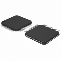
IC UART QUAD W/FIFO 80-LQFP
Manufacturer
NXP Semiconductors
Datasheet
1.SC28L194A1BE528.pdf
(52 pages)
Specifications of SC28L194A1BE,557
Features
False-start Bit Detection
Number Of Channels
4, QUART
Fifo's
16 Byte
Voltage - Supply
3.3V, 5V
With Auto Flow Control
Yes
With False Start Bit Detection
Yes
With Modem Control
Yes
With Cmos
Yes
Mounting Type
Surface Mount
Package / Case
80-LQFP
Lead Free Status / RoHS Status
Lead free / RoHS Compliant
Other names
568-1209
935262730557
SC28L194A1BE
935262730557
SC28L194A1BE
Available stocks
Company
Part Number
Manufacturer
Quantity
Price
Company:

Part Number:
SC28L194A1BE,557
Manufacturer:
NXP Semiconductors
Quantity:
10 000


Philips Semiconductors
AC ELECTRICAL SPECIFICATIONS FOR COMMERCIAL AND INDUSTRIAL (3.3V)
V
2006 Aug 15
Reset Timing
Bus Timing
I/O Port Pin Timing
Interrupt Timing
Tx/Rx Clock Timing
Transmitter Timing
Receiver Timing
CC
SYMBOL
SYMBOL
Quad UART for 3.3 V and 5 V supply voltage
t
t
t
t
t
t
t
t
t
t
t
t
t
t
t
t
t
t
t
t
t
t
f
f
t
f
f
t
t
t
t
ts
RES
AS
AH
t
t
C
CH
STP
RWS
RWH
DD
DF
DS
DH
RWD
PS
PH
PD
PD
IR
IR
DD
RX
RX
TX
TX
TXD
TCS
RXS
RXH
CS
CS
STRT
= 3.3V
4
4
4
4
1
10%, –40 to +85 C
FIG #
FIG. #
RESET pulse width
A0–A7 setup time before Sclk C3 rising edge
A0–A7 hold time after Sclk C3 rising edge
CEN setup time before Sclk C1 high (Async)
CEN setup time before Sclk C2 high (Sync)
CEN hold time after Sclk C3 high (Sync)
CEN hold time after Sclk C4 high (Async)
CEN high before next C2 to stop next cycle (Sync Mode)
W–Rn setup time before Sclk C2 rising edge
W–Rn hold time after Sclk C3 rising edge
Read cycle Data valid after Sclk C3 falling edge
Read cycle data bus floating after CEN high (Async)
Read cycle data bus floating after C4 end (Sync)
Write cycle data setup time before Sclk C4 rising edge
Write cycle data hold time after Sclk C4 rising edge
High time between CEN low (Async)
I/O input setup time before Sclk C3 falling edge (Read IPR)
I/O input hold time after Sclk C4 rising edge
I/O output valid from:
IRQN from:
Interrupt vector valid after C3 rising edge
RxC high or low time
RxC frequency
RxC frequency
TxC high or low time
TxC frequency
TxC frequency
TxD output delay from TxC low
TxC output delay from TxD output data
RxD data setup time to RxC high (data)
RxD data hold time from RxC high (data)
RxD data low time for receiving a valid Start Bit
Write Sclk C4 rising edge (write to IOPIOR)
Internal interrupt source active bid
Reset to IRQN inactive
Write IMR (set or clear IMR bit)
(16 X)
(1 X)
(16 X)
(1 X)
PARAMETER
PARAMETER
3
38
2
17/32
MIN.
–15
10
22
30
25
50
30
25
25
25
15
18
12
22
25
20
25
25
8
8
7
0
0
0
0
1
1
1
LIMITS
1
1
1
1
/
TYP.
/
/
/
2
12
2
2
2
20
17
11
14
14
50
26
60
40
20
50
14
14
Sclk
3
3
3
4
4
8
7
4
Sclk
Sclk
Sclk
SC28L194
MAX.
Product data sheet
40
30
20
80
43
90
60
30
90
15
8
1
8
1
bit time
UNIT
UNIT
MHz
MHz
MHz
MHz
Sclk
Sclk
ns
ns
ns
ns
ns
ns
ns
ns
ns
ns
ns
ns
ns
ns
ns
ns
ns
ns
ns
ns
ns
ns
ns
ns
ns
ns
ns
Related parts for SC28L194A1BE,557
Image
Part Number
Description
Manufacturer
Datasheet
Request
R

Part Number:
Description:
NXP Semiconductors designed the LPC2420/2460 microcontroller around a 16-bit/32-bitARM7TDMI-S CPU core with real-time debug interfaces that include both JTAG andembedded trace
Manufacturer:
NXP Semiconductors
Datasheet:

Part Number:
Description:
NXP Semiconductors designed the LPC2458 microcontroller around a 16-bit/32-bitARM7TDMI-S CPU core with real-time debug interfaces that include both JTAG andembedded trace
Manufacturer:
NXP Semiconductors
Datasheet:
Part Number:
Description:
NXP Semiconductors designed the LPC2468 microcontroller around a 16-bit/32-bitARM7TDMI-S CPU core with real-time debug interfaces that include both JTAG andembedded trace
Manufacturer:
NXP Semiconductors
Datasheet:
Part Number:
Description:
NXP Semiconductors designed the LPC2470 microcontroller, powered by theARM7TDMI-S core, to be a highly integrated microcontroller for a wide range ofapplications that require advanced communications and high quality graphic displays
Manufacturer:
NXP Semiconductors
Datasheet:
Part Number:
Description:
NXP Semiconductors designed the LPC2478 microcontroller, powered by theARM7TDMI-S core, to be a highly integrated microcontroller for a wide range ofapplications that require advanced communications and high quality graphic displays
Manufacturer:
NXP Semiconductors
Datasheet:
Part Number:
Description:
The Philips Semiconductors XA (eXtended Architecture) family of 16-bit single-chip microcontrollers is powerful enough to easily handle the requirements of high performance embedded applications, yet inexpensive enough to compete in the market for hi
Manufacturer:
NXP Semiconductors
Datasheet:
Part Number:
Description:
The XA-S3 device is a member of Philips Semiconductors? XA(eXtended Architecture) family of high performance 16-bitsingle-chip microcontrollers
Manufacturer:
NXP Semiconductors
Datasheet:

Part Number:
Description:
The NXP BlueStreak LH75401/LH75411 family consists of two low-cost 16/32-bit System-on-Chip (SoC) devices
Manufacturer:
NXP Semiconductors
Datasheet:
Part Number:
Description:
The NXP LPC3130/3131 combine an 180 MHz ARM926EJ-S CPU core, high-speed USB2
Manufacturer:
NXP Semiconductors
Datasheet:
Part Number:
Description:
The NXP LPC3141 combine a 270 MHz ARM926EJ-S CPU core, High-speed USB 2
Manufacturer:
NXP Semiconductors
Part Number:
Description:
The NXP LPC3143 combine a 270 MHz ARM926EJ-S CPU core, High-speed USB 2
Manufacturer:
NXP Semiconductors

Part Number:
Description:
The NXP LPC3152 combines an 180 MHz ARM926EJ-S CPU core, High-speed USB 2
Manufacturer:
NXP Semiconductors
Part Number:
Description:
The NXP LPC3154 combines an 180 MHz ARM926EJ-S CPU core, High-speed USB 2
Manufacturer:
NXP Semiconductors

Part Number:
Description:
Standard level N-channel enhancement mode Field-Effect Transistor (FET) in a plastic package using NXP High-Performance Automotive (HPA) TrenchMOS technology
Manufacturer:
NXP Semiconductors
Datasheet: