SC28C94A1A,518 NXP Semiconductors, SC28C94A1A,518 Datasheet - Page 25
SC28C94A1A,518
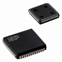
Manufacturer Part Number
SC28C94A1A,518
Description
IC UART QUAD W/FIFO 52-PLCC
Manufacturer
NXP Semiconductors
Datasheet
1.SC28C94A1A518.pdf
(39 pages)
Specifications of SC28C94A1A,518
Features
False-start Bit Detection
Number Of Channels
4, QUART
Fifo's
8 Byte
Voltage - Supply
5V
With Auto Flow Control
Yes
With False Start Bit Detection
Yes
With Modem Control
Yes
With Cmos
Yes
Mounting Type
Surface Mount
Package / Case
52-PLCC
Lead Free Status / RoHS Status
Lead free / RoHS Compliant
Other names
568-1114-2
935262534518
SC28C94A1A-T
935262534518
SC28C94A1A-T
Available stocks
Company
Part Number
Manufacturer
Quantity
Price
Company:

Part Number:
SC28C94A1A,518
Manufacturer:
Maxim
Quantity:
21
Company:
Part Number:
SC28C94A1A,518
Manufacturer:
NXP Semiconductors
Quantity:
10 000


Philips Semiconductors
AC ELECTRICAL CHARACTERISTICS
V
NOTES:
1. All voltage measurements are referenced to ground (GND). For testing, all inputs swing between 0.4 V and 2.4 V with a transition time of
2. Typical values are at +25 C, typical supply voltages, and typical processing parameters.
3. Test condition for interrupt and I/O outputs: C
4. Timing is illustrated and referenced to the WRN and RDN inputs. The device may also be operated with CEN as the ‘strobing’ input. CEN
5. The minimum value is not tested, but is guaranteed by design. For t
2006 Aug 09
Reset timing
t
I/O Port timing
t
t
t
Interrupt timing
t
Clock timing
t
t
t
t
f
t
f
t
f
Transmitter timing
t
t
Receiver timing
t
t
CC
SYMBOL
SYMBOL
RES
PS
PH
PD
IR
CLK
CLK
CLK
CTC
CTC
RX
RX
TX
TX
TXD
TCS
RXS
RXH
Quad universal asynchronous receiver/transmitter (QUART)
20 ns maximum. For X1/CLK this swing is between 0.4 V and 4.4 V. All time measurements are referenced at input voltages of V
as appropriate.
and RDN (also CEN and WRN) are ANDed internally. As a consequence, the signal asserted last initiates the cycle and the signal negated
first terminates the cycle.
5
5
= 5V
5
5
10%, T
FIGURE
FIGURE
10
12
13
13
13
13
13
13
13
13
13
14
14
15
15
11
11
11
A
= –40 C to 85 C, unless otherwise specified.
Reset pulse width
I/O input setup time before RDN Low
I/O input hold time after RDN High
I/O output valid from
IRQN negated or I/O output High from:
X1/CLK low/high time
X1/CLK low/high time (above 4MHz; X1/CLK
X1/CLK frequency
Counter/timer clock high or low time
Counter/timer clock frequency
RxC high or low time
RxC frequency (16X)
RxC frequency (1X)
TxC high or low time
TxC frequency (16X)
TxC frequency (1X)
TxD output delay from TxC low
TxC output delay from TxD output data
RxD data setup time to RxC high
RxD data hold time from RxC high
Reset command (break change interrupt)
Reset command (I/O change interrupt)
Stop C/T command (counter interrupt)
Read RHR (RxRDY/FFULL interrupt)
Write THR (TxRDY interrupt)
Write IMR (clear of interrupt mask bit)
WRN High (WRN or CEN high, whichever occurs first)
RDN Low (RDN or CEN low, whichever occurs last)
L
= 50 pF, R
1, 2, 3, 4
PARAMETER
PARAMETER
L
= 2.7 k to V
25
CLK
2 active)
CC
With respect to a
3.6864MHz clock
on pin X1/CLK
minimum test rate is 2.0 MHz.
. Test conditions for rest of outputs: C
125/100
56/56
Min
200
–10
60
30
30
60
60
0
0
0
0
0
0
0
0
LIMITS
3.6864
Typ
5
5
L
= 150 pF.
Max
+10
8.0
1.0
1.0
40
40
80
80
80
80
80
80
16
16
70
SC28C94
8
Product data sheet
IL
UNIT
UNIT
and V
MHz
MHz
MHz
MHz
MHz
MHz
ns
ns
ns
ns
ns
ns
ns
ns
ns
ns
ns
ns
ns
ns
ns
ns
ns
ns
ns
ns
IH
,
Related parts for SC28C94A1A,518
Image
Part Number
Description
Manufacturer
Datasheet
Request
R

Part Number:
Description:
NXP Semiconductors designed the LPC2420/2460 microcontroller around a 16-bit/32-bitARM7TDMI-S CPU core with real-time debug interfaces that include both JTAG andembedded trace
Manufacturer:
NXP Semiconductors
Datasheet:

Part Number:
Description:
NXP Semiconductors designed the LPC2458 microcontroller around a 16-bit/32-bitARM7TDMI-S CPU core with real-time debug interfaces that include both JTAG andembedded trace
Manufacturer:
NXP Semiconductors
Datasheet:
Part Number:
Description:
NXP Semiconductors designed the LPC2468 microcontroller around a 16-bit/32-bitARM7TDMI-S CPU core with real-time debug interfaces that include both JTAG andembedded trace
Manufacturer:
NXP Semiconductors
Datasheet:
Part Number:
Description:
NXP Semiconductors designed the LPC2470 microcontroller, powered by theARM7TDMI-S core, to be a highly integrated microcontroller for a wide range ofapplications that require advanced communications and high quality graphic displays
Manufacturer:
NXP Semiconductors
Datasheet:
Part Number:
Description:
NXP Semiconductors designed the LPC2478 microcontroller, powered by theARM7TDMI-S core, to be a highly integrated microcontroller for a wide range ofapplications that require advanced communications and high quality graphic displays
Manufacturer:
NXP Semiconductors
Datasheet:
Part Number:
Description:
The Philips Semiconductors XA (eXtended Architecture) family of 16-bit single-chip microcontrollers is powerful enough to easily handle the requirements of high performance embedded applications, yet inexpensive enough to compete in the market for hi
Manufacturer:
NXP Semiconductors
Datasheet:
Part Number:
Description:
The XA-S3 device is a member of Philips Semiconductors? XA(eXtended Architecture) family of high performance 16-bitsingle-chip microcontrollers
Manufacturer:
NXP Semiconductors
Datasheet:

Part Number:
Description:
The NXP BlueStreak LH75401/LH75411 family consists of two low-cost 16/32-bit System-on-Chip (SoC) devices
Manufacturer:
NXP Semiconductors
Datasheet:
Part Number:
Description:
The NXP LPC3130/3131 combine an 180 MHz ARM926EJ-S CPU core, high-speed USB2
Manufacturer:
NXP Semiconductors
Datasheet:
Part Number:
Description:
The NXP LPC3141 combine a 270 MHz ARM926EJ-S CPU core, High-speed USB 2
Manufacturer:
NXP Semiconductors
Part Number:
Description:
The NXP LPC3143 combine a 270 MHz ARM926EJ-S CPU core, High-speed USB 2
Manufacturer:
NXP Semiconductors

Part Number:
Description:
The NXP LPC3152 combines an 180 MHz ARM926EJ-S CPU core, High-speed USB 2
Manufacturer:
NXP Semiconductors
Part Number:
Description:
The NXP LPC3154 combines an 180 MHz ARM926EJ-S CPU core, High-speed USB 2
Manufacturer:
NXP Semiconductors

Part Number:
Description:
Standard level N-channel enhancement mode Field-Effect Transistor (FET) in a plastic package using NXP High-Performance Automotive (HPA) TrenchMOS technology
Manufacturer:
NXP Semiconductors
Datasheet: