SC16C654BIA68,512 NXP Semiconductors, SC16C654BIA68,512 Datasheet - Page 58
SC16C654BIA68,512
Manufacturer Part Number
SC16C654BIA68,512
Description
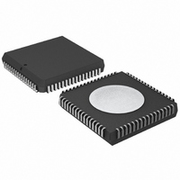
ID QUAD UART 64BYTE 68PLCC
Manufacturer
NXP Semiconductors
Datasheet
1.SC16C654BIBS528.pdf
(58 pages)
Specifications of SC16C654BIA68,512
Features
False-start Bit Detection
Number Of Channels
4, QUART
Fifo's
64 Byte
Voltage - Supply
2.5V, 3.3V, 5V
With Auto Flow Control
Yes
With Irda Encoder/decoder
Yes
With False Start Bit Detection
Yes
With Modem Control
Yes
With Cmos
Yes
Mounting Type
Surface Mount
Package / Case
68-LCC (J-Lead)
Transmit Fifo
64Byte
Receive Fifo
64Byte
Transmitter And Receiver Fifo Counter
Yes
Data Rate
5Mbps
Package Type
PLCC
Operating Supply Voltage (max)
5.5V
Mounting
Surface Mount
Operating Temperature (min)
-40C
Operating Temperature (max)
85C
Operating Temperature Classification
Industrial
Lead Free Status / RoHS Status
Lead free / RoHS Compliant
Other names
935274935512
SC16C654BIA68
SC16C654BIA68
SC16C654BIA68
SC16C654BIA68
Available stocks
Company
Part Number
Manufacturer
Quantity
Price
Company:

Part Number:
SC16C654BIA68,512
Manufacturer:
NXP Semiconductors
Quantity:
10 000


Philips Semiconductors
20. Contents
1
2
3
4
5
5.1
5.2
6
6.1
6.1.1
6.1.2
6.2
6.3
6.4
6.5
6.6
6.7
6.8
6.9
6.10
6.11
6.12
7
7.1
7.2
7.2.1
7.2.2
7.3
7.3.1
7.3.1.1
7.3.1.2
7.3.2
7.4
7.5
7.6
7.7
7.8
7.9
7.10
7.11
8
9
10
General description . . . . . . . . . . . . . . . . . . . . . . 1
Features . . . . . . . . . . . . . . . . . . . . . . . . . . . . . . . 1
Ordering information . . . . . . . . . . . . . . . . . . . . . 2
Block diagram . . . . . . . . . . . . . . . . . . . . . . . . . . 3
Pinning information . . . . . . . . . . . . . . . . . . . . . . 5
Functional description . . . . . . . . . . . . . . . . . . 14
Register descriptions . . . . . . . . . . . . . . . . . . . 24
Limiting values. . . . . . . . . . . . . . . . . . . . . . . . . 37
Static characteristics. . . . . . . . . . . . . . . . . . . . 38
Dynamic characteristics . . . . . . . . . . . . . . . . . 39
Pinning . . . . . . . . . . . . . . . . . . . . . . . . . . . . . . . 5
Pin description . . . . . . . . . . . . . . . . . . . . . . . . 10
Interface options . . . . . . . . . . . . . . . . . . . . . . . 16
The 16 mode interface . . . . . . . . . . . . . . . . . . 16
The 68 mode interface . . . . . . . . . . . . . . . . . . 16
Internal registers. . . . . . . . . . . . . . . . . . . . . . . 17
FIFO operation . . . . . . . . . . . . . . . . . . . . . . . . 17
Hardware flow control . . . . . . . . . . . . . . . . . . . 18
Software flow control . . . . . . . . . . . . . . . . . . . 18
Special feature software flow control . . . . . . . 19
Xon any feature . . . . . . . . . . . . . . . . . . . . . . . 19
Hardware/software and time-out interrupts. . . 19
Programmable baud rate generator . . . . . . . . 20
DMA operation . . . . . . . . . . . . . . . . . . . . . . . . 22
Sleep mode. . . . . . . . . . . . . . . . . . . . . . . . . . . 22
Loop-back mode . . . . . . . . . . . . . . . . . . . . . . . 22
Transmit (THR) and Receive (RHR) Holding
Registers. . . . . . . . . . . . . . . . . . . . . . . . . . . . . 25
Interrupt Enable Register (IER) . . . . . . . . . . . 25
IER versus Receive FIFO interrupt mode
operation. . . . . . . . . . . . . . . . . . . . . . . . . . . . . 26
IER versus Receive/Transmit FIFO polled mode
operation. . . . . . . . . . . . . . . . . . . . . . . . . . . . . 26
FIFO Control Register (FCR) . . . . . . . . . . . . . 27
DMA mode . . . . . . . . . . . . . . . . . . . . . . . . . . . 27
Mode 0 (FCR bit 3 = 0) . . . . . . . . . . . . . . . . . . 27
Mode 1 (FCR bit 3 = 1) . . . . . . . . . . . . . . . . . . 27
FIFO mode . . . . . . . . . . . . . . . . . . . . . . . . . . . 27
Interrupt Status Register (ISR) . . . . . . . . . . . . 29
Line Control Register (LCR) . . . . . . . . . . . . . . 30
Modem Control Register (MCR) . . . . . . . . . . . 31
Line Status Register (LSR) . . . . . . . . . . . . . . . 33
Modem Status Register (MSR). . . . . . . . . . . . 34
Scratchpad Register (SPR) . . . . . . . . . . . . . . 35
Enhanced Feature Register (EFR) . . . . . . . . . 35
SC16C654B/654DB external reset conditions 36
5 V, 3.3 V and 2.5 V quad UART, 5 Mbit/s (max.) with 64-byte FIFOs
10.1
11
12
12.1
12.2
12.3
12.4
12.5
13
14
15
16
17
18
19
© Koninklijke Philips Electronics N.V. 2005
All rights are reserved. Reproduction in whole or in part is prohibited without the prior
written consent of the copyright owner. The information presented in this document does
not form part of any quotation or contract, is believed to be accurate and reliable and may
be changed without notice. No liability will be accepted by the publisher for any
consequence of its use. Publication thereof does not convey nor imply any license under
patent- or other industrial or intellectual property rights.
Published in The Netherlands
Package outline . . . . . . . . . . . . . . . . . . . . . . . . 48
Soldering . . . . . . . . . . . . . . . . . . . . . . . . . . . . . 53
Abbreviations . . . . . . . . . . . . . . . . . . . . . . . . . 55
Revision history . . . . . . . . . . . . . . . . . . . . . . . 56
Data sheet status. . . . . . . . . . . . . . . . . . . . . . . 57
Definitions . . . . . . . . . . . . . . . . . . . . . . . . . . . . 57
Disclaimers . . . . . . . . . . . . . . . . . . . . . . . . . . . 57
Trademarks . . . . . . . . . . . . . . . . . . . . . . . . . . . 57
Contact information . . . . . . . . . . . . . . . . . . . . 57
Timing diagrams. . . . . . . . . . . . . . . . . . . . . . . 41
Introduction to soldering surface mount
packages . . . . . . . . . . . . . . . . . . . . . . . . . . . . 53
Reflow soldering. . . . . . . . . . . . . . . . . . . . . . . 53
Wave soldering. . . . . . . . . . . . . . . . . . . . . . . . 53
Manual soldering . . . . . . . . . . . . . . . . . . . . . . 54
Package related soldering information . . . . . . 54
SC16C654B/654DB
Document number: 9397 750 14965
Date of release: 20 June 2005
Related parts for SC16C654BIA68,512
Image
Part Number
Description
Manufacturer
Datasheet
Request
R

Part Number:
Description:
NXP Semiconductors designed the LPC2420/2460 microcontroller around a 16-bit/32-bitARM7TDMI-S CPU core with real-time debug interfaces that include both JTAG andembedded trace
Manufacturer:
NXP Semiconductors
Datasheet:

Part Number:
Description:
NXP Semiconductors designed the LPC2458 microcontroller around a 16-bit/32-bitARM7TDMI-S CPU core with real-time debug interfaces that include both JTAG andembedded trace
Manufacturer:
NXP Semiconductors
Datasheet:
Part Number:
Description:
NXP Semiconductors designed the LPC2468 microcontroller around a 16-bit/32-bitARM7TDMI-S CPU core with real-time debug interfaces that include both JTAG andembedded trace
Manufacturer:
NXP Semiconductors
Datasheet:
Part Number:
Description:
NXP Semiconductors designed the LPC2470 microcontroller, powered by theARM7TDMI-S core, to be a highly integrated microcontroller for a wide range ofapplications that require advanced communications and high quality graphic displays
Manufacturer:
NXP Semiconductors
Datasheet:
Part Number:
Description:
NXP Semiconductors designed the LPC2478 microcontroller, powered by theARM7TDMI-S core, to be a highly integrated microcontroller for a wide range ofapplications that require advanced communications and high quality graphic displays
Manufacturer:
NXP Semiconductors
Datasheet:
Part Number:
Description:
The Philips Semiconductors XA (eXtended Architecture) family of 16-bit single-chip microcontrollers is powerful enough to easily handle the requirements of high performance embedded applications, yet inexpensive enough to compete in the market for hi
Manufacturer:
NXP Semiconductors
Datasheet:
Part Number:
Description:
The XA-S3 device is a member of Philips Semiconductors? XA(eXtended Architecture) family of high performance 16-bitsingle-chip microcontrollers
Manufacturer:
NXP Semiconductors
Datasheet:

Part Number:
Description:
The NXP BlueStreak LH75401/LH75411 family consists of two low-cost 16/32-bit System-on-Chip (SoC) devices
Manufacturer:
NXP Semiconductors
Datasheet:
Part Number:
Description:
The NXP LPC3130/3131 combine an 180 MHz ARM926EJ-S CPU core, high-speed USB2
Manufacturer:
NXP Semiconductors
Datasheet:
Part Number:
Description:
The NXP LPC3141 combine a 270 MHz ARM926EJ-S CPU core, High-speed USB 2
Manufacturer:
NXP Semiconductors
Part Number:
Description:
The NXP LPC3143 combine a 270 MHz ARM926EJ-S CPU core, High-speed USB 2
Manufacturer:
NXP Semiconductors

Part Number:
Description:
The NXP LPC3152 combines an 180 MHz ARM926EJ-S CPU core, High-speed USB 2
Manufacturer:
NXP Semiconductors
Part Number:
Description:
The NXP LPC3154 combines an 180 MHz ARM926EJ-S CPU core, High-speed USB 2
Manufacturer:
NXP Semiconductors

Part Number:
Description:
Standard level N-channel enhancement mode Field-Effect Transistor (FET) in a plastic package using NXP High-Performance Automotive (HPA) TrenchMOS technology
Manufacturer:
NXP Semiconductors
Datasheet: