SC16IS760IBS,151 NXP Semiconductors, SC16IS760IBS,151 Datasheet - Page 42
SC16IS760IBS,151
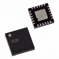
Manufacturer Part Number
SC16IS760IBS,151
Description
IC UART I2C/SPI 24-HVQFN
Manufacturer
NXP Semiconductors
Type
IrDA or RS- 232 or RS- 485r
Datasheet
1.SC16IS740IPW112.pdf
(62 pages)
Specifications of SC16IS760IBS,151
Number Of Channels
1, UART
Package / Case
24-VQFN Exposed Pad, 24-HVQFN, 24-SQFN, 24-DHVQFN
Features
Low Current
Fifo's
64 Byte
Protocol
RS232, RS485
Voltage - Supply
2.5V, 3.3V, 5V
With Auto Flow Control
Yes
With False Start Bit Detection
Yes
With Modem Control
Yes
Mounting Type
Surface Mount
Data Rate
5 Mbps
Supply Voltage (max)
3.6 V
Supply Voltage (min)
2.3 V
Supply Current
6 mA
Maximum Operating Temperature
+ 85 C
Minimum Operating Temperature
- 40 C
Mounting Style
SMD/SMT
Operating Supply Voltage
2.5 V or 3.3 V
Lead Free Status / RoHS Status
Lead free / RoHS Compliant
For Use With
568-4000 - DEMO BOARD SPI/I2C TO DUAL UART568-3510 - DEMO BOARD SPI/I2C TO UART
Lead Free Status / Rohs Status
Lead free / RoHS Compliant
Other names
568-2238
935279279151
SC16IS760IBS-S
935279279151
SC16IS760IBS-S


NXP Semiconductors
SC16IS740_750_760_6
Product data sheet
Fig 22. Master writes to slave
Fig 23. Master read from slave
(1) See
(1) See
S
White block: host to SC16IS740/750/760
Grey block: SC16IS740/750/760 to host
White block: host to SC16IS740/750/760
Grey block: SC16IS740/750/760 to host
SLAVE ADDRESS
Table 33
Table 33
S
for additional information.
for additional information.
SLAVE ADDRESS
Table 33
SPI interfaces. Bit 0 is not used, bits 2:1 select the channel, bits 6:3 select one of the
UART internal registers. Bit 7 is not used with the I
SPI interface to indicate a read or a write operation.
The register read cycle (see
sending a slave address with the direction bit set to ‘write’ with a following subaddress.
Then, in order to reverse the direction of the transfer, the master issues a repeated START
followed again by the device address, but this time with the direction bit set to ‘read’. The
data bytes starting at the internal subaddress will be clocked out of the device, each
followed by a master-generated acknowledge. The last byte of the read cycle will be
followed by a negative acknowledge, signalling the end of transfer. The cycle is terminated
by a STOP signal.
Table 33.
Bit
7
6:3
2:1
0
W
and
Register address byte (I
Name
-
A[3:0]
CH1, CH0
-
Table 34
A
W
REGISTER ADDRESS
Single UART with I
show the bits’ presentation at the subaddress byte for I
A
Rev. 06 — 13 May 2008
REGISTER ADDRESS
Figure
Function
not used
UART’s internal register select
channel select: CH1 = 0, CH0 = 0
Other values are reserved and should not be used.
not used
2
(1)
C)
23) commences in a similar manner, with the master
A
2
C-bus/SPI interface, 64-byte FIFOs, IrDA SIR
nDATA
(1)
S
SC16IS740/750/760
A
2
C-bus interface, but it is used by the
SLAVE ADDRESS
A
nDATA
LAST DATA
A
002aab047
R
© NXP B.V. 2008. All rights reserved.
P
NA
A
2
002aab048
C-bus and
P
42 of 62
Related parts for SC16IS760IBS,151
Image
Part Number
Description
Manufacturer
Datasheet
Request
R

Part Number:
Description:
Single UART with I2C-bus/SPI interface
Manufacturer:
NXP Semiconductors
Datasheet:
Part Number:
Description:
NXP Semiconductors designed the LPC2420/2460 microcontroller around a 16-bit/32-bitARM7TDMI-S CPU core with real-time debug interfaces that include both JTAG andembedded trace
Manufacturer:
NXP Semiconductors
Datasheet:

Part Number:
Description:
NXP Semiconductors designed the LPC2458 microcontroller around a 16-bit/32-bitARM7TDMI-S CPU core with real-time debug interfaces that include both JTAG andembedded trace
Manufacturer:
NXP Semiconductors
Datasheet:
Part Number:
Description:
NXP Semiconductors designed the LPC2468 microcontroller around a 16-bit/32-bitARM7TDMI-S CPU core with real-time debug interfaces that include both JTAG andembedded trace
Manufacturer:
NXP Semiconductors
Datasheet:
Part Number:
Description:
NXP Semiconductors designed the LPC2470 microcontroller, powered by theARM7TDMI-S core, to be a highly integrated microcontroller for a wide range ofapplications that require advanced communications and high quality graphic displays
Manufacturer:
NXP Semiconductors
Datasheet:
Part Number:
Description:
NXP Semiconductors designed the LPC2478 microcontroller, powered by theARM7TDMI-S core, to be a highly integrated microcontroller for a wide range ofapplications that require advanced communications and high quality graphic displays
Manufacturer:
NXP Semiconductors
Datasheet:
Part Number:
Description:
The Philips Semiconductors XA (eXtended Architecture) family of 16-bit single-chip microcontrollers is powerful enough to easily handle the requirements of high performance embedded applications, yet inexpensive enough to compete in the market for hi
Manufacturer:
NXP Semiconductors
Datasheet:
Part Number:
Description:
The XA-S3 device is a member of Philips Semiconductors? XA(eXtended Architecture) family of high performance 16-bitsingle-chip microcontrollers
Manufacturer:
NXP Semiconductors
Datasheet:

Part Number:
Description:
The NXP BlueStreak LH75401/LH75411 family consists of two low-cost 16/32-bit System-on-Chip (SoC) devices
Manufacturer:
NXP Semiconductors
Datasheet:
Part Number:
Description:
The NXP LPC3130/3131 combine an 180 MHz ARM926EJ-S CPU core, high-speed USB2
Manufacturer:
NXP Semiconductors
Datasheet:
Part Number:
Description:
The NXP LPC3141 combine a 270 MHz ARM926EJ-S CPU core, High-speed USB 2
Manufacturer:
NXP Semiconductors
Part Number:
Description:
The NXP LPC3143 combine a 270 MHz ARM926EJ-S CPU core, High-speed USB 2
Manufacturer:
NXP Semiconductors

Part Number:
Description:
The NXP LPC3152 combines an 180 MHz ARM926EJ-S CPU core, High-speed USB 2
Manufacturer:
NXP Semiconductors
Part Number:
Description:
The NXP LPC3154 combines an 180 MHz ARM926EJ-S CPU core, High-speed USB 2
Manufacturer:
NXP Semiconductors