SC16IS760IBS,151 NXP Semiconductors, SC16IS760IBS,151 Datasheet - Page 37
SC16IS760IBS,151
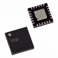
Manufacturer Part Number
SC16IS760IBS,151
Description
IC UART I2C/SPI 24-HVQFN
Manufacturer
NXP Semiconductors
Type
IrDA or RS- 232 or RS- 485r
Datasheet
1.SC16IS740IPW112.pdf
(62 pages)
Specifications of SC16IS760IBS,151
Number Of Channels
1, UART
Package / Case
24-VQFN Exposed Pad, 24-HVQFN, 24-SQFN, 24-DHVQFN
Features
Low Current
Fifo's
64 Byte
Protocol
RS232, RS485
Voltage - Supply
2.5V, 3.3V, 5V
With Auto Flow Control
Yes
With False Start Bit Detection
Yes
With Modem Control
Yes
Mounting Type
Surface Mount
Data Rate
5 Mbps
Supply Voltage (max)
3.6 V
Supply Voltage (min)
2.3 V
Supply Current
6 mA
Maximum Operating Temperature
+ 85 C
Minimum Operating Temperature
- 40 C
Mounting Style
SMD/SMT
Operating Supply Voltage
2.5 V or 3.3 V
Lead Free Status / RoHS Status
Lead free / RoHS Compliant
For Use With
568-4000 - DEMO BOARD SPI/I2C TO DUAL UART568-3510 - DEMO BOARD SPI/I2C TO UART
Lead Free Status / Rohs Status
Lead free / RoHS Compliant
Other names
568-2238
935279279151
SC16IS760IBS-S
935279279151
SC16IS760IBS-S


NXP Semiconductors
10. I
SC16IS740_750_760_6
Product data sheet
2
C-bus operation
10.1 Data transfers
The two lines of the I
lines are connected to a positive supply via a pull-up resistor, and remain HIGH when the
bus is not busy. Each device is recognized by a unique address whether it is a
microcomputer, LCD driver, memory or keyboard interface and can operate as either a
transmitter or receiver, depending on the function of the device. A device generating a
message or data is a transmitter, and a device receiving the message or data is a
receiver. Obviously, a passive function like an LCD driver could only be a receiver, while a
microcontroller or a memory can both transmit and receive data.
One data bit is transferred during each clock pulse (see
line must remain stable during the HIGH period of the clock pulse in order to be valid.
Changes in the data line at this time will be interpreted as control signals. A HIGH-to-LOW
transition of the data line (SDA) while the clock signal (SCL) is HIGH indicates a START
condition, and a LOW-to-HIGH transition of the SDA while SCL is HIGH defines a STOP
condition (see
free again at a certain time interval after the STOP condition. The START and STOP
conditions are always generated by the master.
The number of data bytes transferred between the START and STOP condition from
transmitter to receiver is not limited. Each byte, which must be eight bits long, is
transferred serially with the most significant bit first, and is followed by an acknowledge bit
(see
master. The device that acknowledges has to pull down the SDA line during the
acknowledge clock pulse, while the transmitting device releases this pulse (see
Figure
Fig 16. Bit transfer on the I
Fig 17. START and STOP conditions
Figure
SDA
SCL
19).
18). The clock pulse related to the acknowledge bit is generated by the
Figure
START condition
SDA
SCL
S
2
Single UART with I
C-bus are a serial data line (SDA) and a serial clock line (SCL). Both
17). The bus is considered to be busy after the START condition and
Rev. 06 — 13 May 2008
2
C-bus
data valid
data line
stable;
2
C-bus/SPI interface, 64-byte FIFOs, IrDA SIR
allowed
change
of data
SC16IS740/750/760
Figure
STOP condition
16). The data on the SDA
mba607
P
© NXP B.V. 2008. All rights reserved.
mba608
SDA
SCL
37 of 62
Related parts for SC16IS760IBS,151
Image
Part Number
Description
Manufacturer
Datasheet
Request
R

Part Number:
Description:
Single UART with I2C-bus/SPI interface
Manufacturer:
NXP Semiconductors
Datasheet:
Part Number:
Description:
NXP Semiconductors designed the LPC2420/2460 microcontroller around a 16-bit/32-bitARM7TDMI-S CPU core with real-time debug interfaces that include both JTAG andembedded trace
Manufacturer:
NXP Semiconductors
Datasheet:

Part Number:
Description:
NXP Semiconductors designed the LPC2458 microcontroller around a 16-bit/32-bitARM7TDMI-S CPU core with real-time debug interfaces that include both JTAG andembedded trace
Manufacturer:
NXP Semiconductors
Datasheet:
Part Number:
Description:
NXP Semiconductors designed the LPC2468 microcontroller around a 16-bit/32-bitARM7TDMI-S CPU core with real-time debug interfaces that include both JTAG andembedded trace
Manufacturer:
NXP Semiconductors
Datasheet:
Part Number:
Description:
NXP Semiconductors designed the LPC2470 microcontroller, powered by theARM7TDMI-S core, to be a highly integrated microcontroller for a wide range ofapplications that require advanced communications and high quality graphic displays
Manufacturer:
NXP Semiconductors
Datasheet:
Part Number:
Description:
NXP Semiconductors designed the LPC2478 microcontroller, powered by theARM7TDMI-S core, to be a highly integrated microcontroller for a wide range ofapplications that require advanced communications and high quality graphic displays
Manufacturer:
NXP Semiconductors
Datasheet:
Part Number:
Description:
The Philips Semiconductors XA (eXtended Architecture) family of 16-bit single-chip microcontrollers is powerful enough to easily handle the requirements of high performance embedded applications, yet inexpensive enough to compete in the market for hi
Manufacturer:
NXP Semiconductors
Datasheet:
Part Number:
Description:
The XA-S3 device is a member of Philips Semiconductors? XA(eXtended Architecture) family of high performance 16-bitsingle-chip microcontrollers
Manufacturer:
NXP Semiconductors
Datasheet:

Part Number:
Description:
The NXP BlueStreak LH75401/LH75411 family consists of two low-cost 16/32-bit System-on-Chip (SoC) devices
Manufacturer:
NXP Semiconductors
Datasheet:
Part Number:
Description:
The NXP LPC3130/3131 combine an 180 MHz ARM926EJ-S CPU core, high-speed USB2
Manufacturer:
NXP Semiconductors
Datasheet:
Part Number:
Description:
The NXP LPC3141 combine a 270 MHz ARM926EJ-S CPU core, High-speed USB 2
Manufacturer:
NXP Semiconductors
Part Number:
Description:
The NXP LPC3143 combine a 270 MHz ARM926EJ-S CPU core, High-speed USB 2
Manufacturer:
NXP Semiconductors

Part Number:
Description:
The NXP LPC3152 combines an 180 MHz ARM926EJ-S CPU core, High-speed USB 2
Manufacturer:
NXP Semiconductors
Part Number:
Description:
The NXP LPC3154 combines an 180 MHz ARM926EJ-S CPU core, High-speed USB 2
Manufacturer:
NXP Semiconductors