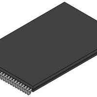
MC74LCX16245DT ON Semiconductor, MC74LCX16245DT Datasheet - Page 4

MC74LCX16245DT
Manufacturer Part Number
MC74LCX16245DT
Description
Bus Transceivers Low Voltage CMOS
Manufacturer
ON Semiconductor
Datasheet
1.MC74LCX16245DT.pdf
(8 pages)
Specifications of MC74LCX16245DT
Logic Type
CMOS
Logic Family
74LCX
Number Of Channels Per Chip
16
Input Level
LVTTL, TTL
Output Level
LVCMOS
Output Type
3-State
High Level Output Current
- 24 mA
Low Level Output Current
24 mA
Propagation Delay Time
5.2 ns
Supply Voltage (max)
3.6 V
Supply Voltage (min)
2 V
Maximum Operating Temperature
+ 85 C
Package / Case
TSSOP-48
Function
Bus Transceiver
Maximum Power Dissipation
200 mW
Minimum Operating Temperature
- 40 C
Mounting Style
SMD/SMT
Number Of Circuits
2
Polarity
Non-Inverting
Lead Free Status / Rohs Status
No RoHS Version Available
Available stocks
Company
Part Number
Manufacturer
Quantity
Price
Company:
Part Number:
MC74LCX16245DT
Manufacturer:
MOT
Quantity:
6 227
Company:
Part Number:
MC74LCX16245DTG
Manufacturer:
ON Semiconductor
Quantity:
1
Part Number:
MC74LCX16245DTG
Manufacturer:
ON/安森美
Quantity:
20 000
Part Number:
MC74LCX16245DTR2
Manufacturer:
ON/安森美
Quantity:
20 000
Company:
Part Number:
MC74LCX16245DTR2G
Manufacturer:
NXP
Quantity:
12 000
Part Number:
MC74LCX16245DTR2G
Manufacturer:
ON/安森美
Quantity:
20 000
Company:
Part Number:
MC74LCX16245DTRG
Manufacturer:
ONSemi
Quantity:
6 876
2. These values of V
3. Skew is defined as the absolute value of the difference between the actual propagation delay for any two separate outputs of the same device.
DC ELECTRICAL CHARACTERISTICS
AC CHARACTERISTICS
Symbol
Symbol
t
t
DI
V
I
t
t
t
t
OSHL
OSLH
V
t
t
The specification applies to any outputs switching in the same direction, either HIGH−to−LOW (t
guaranteed by design.
V
I
V
I
OFF
PLH
PHL
PZH
PHZ
PZL
PLZ
OZ
CC
OH
OL
I
IH
CC
IL
I
HIGH Level Input Voltage (Note 2)
LOW Level Input Voltage (Note 2)
HIGH Level Output Voltage
LOW Level Output Voltage
Input Leakage Current
3−State Output Current
Power−Off Leakage Current
Quiescent Supply Current
Increase in I
Propagation Delay
Input to Output
Output Enable Time to
High and Low Level
Output Disable Time From
High and Low Level
Output−to−Output Skew
(Note 3)
I
Parameter
are used to test DC electrical characteristics only.
CC
Characteristic
per Input
t
R
= t
F
= 2.5 ns; R
Waveform
L
= 500 W
1
2
2
MC74LCX16245
http://onsemi.com
V
2.3 ≤ V
CC
Min
2.3 V ≤ V
2.3 ≤ V
1.5
1.5
1.5
1.5
1.5
1.5
2.3 ≤ V
2.3 ≤ V
2.3 V ≤ V
2.3 V ≤ V
C
= 3.3 V ± 0.3 V
L
V
V
V
V
CC
= 50 pF
V
V
V
V
CC
CC
CC
CC
4
V
CC
CC
CC
CC
CC
CC
CC
CC
2.3 V ≤ V
2.7 V ≤ V
2.3 V ≤ V
2.7 V ≤ V
≤ 3.6 V; 3.6 ≤ V
CC
= 0 V; V
= 2.7 V; I
= 3.0 V; I
= 3.0 V; I
= 2.3 V; I
= 3.0 V; I
= 3.0 V; I
≤ 3.6 V; V
CC
CC
= 2.7 V; I
≤ 3.6 V; V
V
≤ 3.6 V; 0V ≤ V
= 2.3 V; I
Max
4.5
4.5
6.5
6.5
6.4
6.4
1.0
1.0
I
≤ 3.6 V; 0 V ≤ V
Condition
= V
≤ 3.6 V; I
≤ 3.6 V; I
IH
I
CC
CC
CC
CC
or V
OH
OH
OH
OH
OL
OL
or V
OL
IH
OL
I
T
≤ 2.7 V
≤ 3.6 V
≤ 2.7 V
≤ 3.6 V
= GND or V
A
= −12 mA
= −18 mA
= −24 mA
= 12 mA
= 16 mA
= 24 mA
= −8 mA
O
= V
OL
OL
= 8 mA
Min
= −40°C to +85°C
1.5
1.5
1.5
1.5
1.5
1.5
I
IL
= 5.5 V
or V
V
C
= 100 mA
= 100 mA
O
CC
CC
L
I
≤ 5.5 V;
= 50 pF
O
≤ 5.5 V
− 0.6 V
= 2.7 V
≤ 5.5 V
CC
OSHL
Max
5.2
5.2
7.2
7.2
6.9
6.9
) or LOW−to−HIGH (t
V
T
CC
A
Min
V
1.7
2.0
1.8
2.2
2.4
2.2
= −40°C to +85°C
CC
− 0.2
Min
1.5
1.5
1.5
1.5
1.5
1.5
C
= 2.5 V ± 0.2 V
L
= 30 pF
Max
0.55
±5.0
±5.0
±20
500
0.7
0.8
0.2
0.6
0.4
0.4
Max
10
20
5.4
5.4
8.5
8.5
7.7
7.7
OSLH
); parameter
Unit
Unit
mA
mA
mA
mA
mA
mA
ns
ns
ns
ns
V
V
V
V


