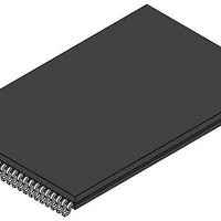
MC74LCX16245DT ON Semiconductor, MC74LCX16245DT Datasheet - Page 2

MC74LCX16245DT
Manufacturer Part Number
MC74LCX16245DT
Description
Bus Transceivers Low Voltage CMOS
Manufacturer
ON Semiconductor
Datasheet
1.MC74LCX16245DT.pdf
(8 pages)
Specifications of MC74LCX16245DT
Logic Type
CMOS
Logic Family
74LCX
Number Of Channels Per Chip
16
Input Level
LVTTL, TTL
Output Level
LVCMOS
Output Type
3-State
High Level Output Current
- 24 mA
Low Level Output Current
24 mA
Propagation Delay Time
5.2 ns
Supply Voltage (max)
3.6 V
Supply Voltage (min)
2 V
Maximum Operating Temperature
+ 85 C
Package / Case
TSSOP-48
Function
Bus Transceiver
Maximum Power Dissipation
200 mW
Minimum Operating Temperature
- 40 C
Mounting Style
SMD/SMT
Number Of Circuits
2
Polarity
Non-Inverting
Lead Free Status / Rohs Status
No RoHS Version Available
Available stocks
Company
Part Number
Manufacturer
Quantity
Price
Company:
Part Number:
MC74LCX16245DT
Manufacturer:
MOT
Quantity:
6 227
Company:
Part Number:
MC74LCX16245DTG
Manufacturer:
ON Semiconductor
Quantity:
1
Part Number:
MC74LCX16245DTG
Manufacturer:
ON/安森美
Quantity:
20 000
Part Number:
MC74LCX16245DTR2
Manufacturer:
ON/安森美
Quantity:
20 000
Company:
Part Number:
MC74LCX16245DTR2G
Manufacturer:
NXP
Quantity:
12 000
Part Number:
MC74LCX16245DTR2G
Manufacturer:
ON/安森美
Quantity:
20 000
Company:
Part Number:
MC74LCX16245DTRG
Manufacturer:
ONSemi
Quantity:
6 876
H
L
Z
X
TRUTH TABLE
OE1
H
L
L
= High Voltage Level
= Low Voltage Level
= High Impedance State
= High or Low Voltage Level and Transitions Are Acceptable; for I
Inputs
Figure 1. Pinout: 48−Lead (Top View)
T/R1
T/R1
GND
GND
GND
GND
T/R2
H
X
L
V
V
B10
B11
B12
B13
B14
B15
B0
B1
B2
B3
CC
B4
B5
B6
B7
B8
B9
CC
10
11
12
13
14
15
16
17
18
19
20
21
22
23
24
1
2
3
4
5
6
7
8
9
Bus B0:7 Data to Bus A0:7
Bus A0:7 Data to Bus B0:7
High Z State on A0:7, B0:7
Outputs
48
47
46
45
44
43
42
41
40
39
38
37
36
35
34
33
32
31
30
29
28
27
26
25
OE1
A0
A1
GND
A2
A3
V
A4
A5
GND
A6
A7
A8
A9
GND
A10
A11
V
A12
A13
GND
A14
A15
OE2
CC
CC
MC74LCX16245
http://onsemi.com
2
CC
OE2
T/R1
Table 1. PIN NAMES
OEn
T/Rn
A0 − A15
B0 − B15
H
reasons, DO NOT FLOAT Inputs
L
L
OE1
A0:7
Inputs
1
48
Pins
T/R2
H
L
X
Figure 2. Logic Diagram
Output Enable Inputs
Transmit/Receive Inputs
Side A Inputs or 3−State Outputs
Side B Inputs or 3−State Outputs
B0:7
Bus B8:15 Data to Bus A8:15
Bus A8:15 Data to Bus B8:15
High Z State on A8:15, B8:15
T/R2
Outputs
A8:15
Function
24
OE2
25
One of Eight
B8:15


