DS90CF581MTD National Semiconductor, DS90CF581MTD Datasheet
DS90CF581MTD
Specifications of DS90CF581MTD
Available stocks


Related parts for DS90CF581MTD

DS90CF581MTD Summary of contents
Page 1
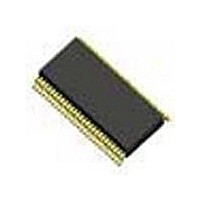
... Power-down mode ■ PLL requires no external components ■ Low profile 56-lead TSSOP package ■ Falling edge data strobe ■ Compatible with TIA/EIA-644 LVDS standard DS90CF581 Order Number DS90CF581MTD See NS Package Number MTD56 12486 Print Date/Time: 2009/10/26 14:44:32 OBSOLETE October 26, 2009 1248628 www.national.com ...
Page 2
Connection Diagram www.national.com Application DS90CF581 2 12486 Version 6 Revision 2 Print Date/Time: 2009/10/26 14:44:32 1248602 1248603 ...
Page 3
... Absolute Maximum Ratings If Military/Aerospace specified devices are required, please contact the National Semiconductor Sales Office/ Distributors for availability and specifications. Supply Voltage ( CMOS/TTL Input Voltage −0 LVDS Driver Output Voltage −0 LVDS Output Short Circuit Duration Junction Temperature Storage Temperature Range Lead Temperature (Soldering, 4 sec ...
Page 4
Note 1: “Absolute Maximum Ratings” are those values beyond which the safety of the device cannot be guaranteed. They are not meant to imply that the device should be operated at these limits. The tables of “Electrical Characteristics” specify conditions ...
Page 5
AC Timing Diagrams Note 7: The worst case test pattern produces a maximum toggling of digital circuits, LVDS I/O and CMOS/TTL I/O. Note 8: The 16 grayscale test pattern tests device power consumption for a “typical” LCD display pattern. The ...
Page 6
FIGURE 3. DS90CF581 (Transmitter) LVDS Output Load and Transition Timing FIGURE 4. DS90CF581 (Transmitter) Input Clock Transition Time Note 11: Measurements diff Note 12: TCCS measured between earliest and latest initial LVDS edges. → Note 13: ...
Page 7
FIGURE 6. DS90CF581 (Transmitter) Setup/Hold and High/Low Times FIGURE 7. DS90CF581 (Transmitter) Clock In to Clock Out Delay FIGURE 8. DS90CF581 (Transmitter) Phase Lock Loop Set Time 7 12486 Version 6 Revision 2 Print Date/Time: 2009/10/26 14:44:32 1248612 1248619 1248614 ...
Page 8
FIGURE 9. 28 Parallel TTL Data Inputs Mapped to LVDS Outputs (DS90CF581) www.national.com FIGURE 10. Transmitter Powerdown Delay 8 12486 Version 6 Revision 2 Print Date/Time: 2009/10/26 14:44:32 1248623 1248624 ...
Page 9
FIGURE 11. Transmitter LVDS Output Pulse Position Measurement DS90CF581 Pin Descriptions —FPD Link Transmitter Pin Name I TxIN I 28 TTL level input. This includes: 8 Red, 8 Green, 8 Blue, and 4 control lines (FPLINE, FPFRAME, DRDY, ...
Page 10
... Physical Dimensions 56-Lead Molded Thin Shrink Small Outline Package, JEDEC www.national.com inches (millimeters) unless otherwise noted Order Number DS90CF581MTD NS Package Number MTD56 10 12486 Version 6 Revision 2 Print Date/Time: 2009/10/26 14:44:32 ...
Page 11
Notes 11 12486 Version 6 Revision 2 Print Date/Time: 2009/10/26 14:44:32 www.national.com ...
Page 12
... For more National Semiconductor product information and proven design tools, visit the following Web sites at: Products Amplifiers www.national.com/amplifiers Audio www.national.com/audio Clock and Timing www.national.com/timing Data Converters www.national.com/adc Interface www.national.com/interface LVDS www.national.com/lvds Power Management www.national.com/power Switching Regulators www.national.com/switchers LDOs www.national.com/ldo LED Lighting www ...