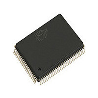
CY7C1297F-117AC Cypress Semiconductor Corp, CY7C1297F-117AC Datasheet

CY7C1297F-117AC
Specifications of CY7C1297F-117AC
Related parts for CY7C1297F-117AC
CY7C1297F-117AC Summary of contents
Page 1
... Supports 3.3V I/O level • Offered in JEDEC-standard 100-pin TQFP • “ZZ” Sleep Mode option Functional Description [1] The CY7C1297F is a 131,072 x 18 synchronous cache RAM designed to interface with high-speed microprocessors with minimum glue logic. Maximum access delay from clock rise is Logic Block Diagram ADDRESS ...
Page 2
... Shaded areas contain advance information. Please contact your local Cypress sales representative for availability of this part. Pin Configuration DDQ DDQ BYTE DDQ DQP DDQ Document #: 38-05429 Rev. *B 133 MHz 117 MHz 6.5 7.5 225 220 40 40 100-Pin TQFP CY7C1297F CY7C1297F Unit DDQ DQP DDQ BYTE DDQ DDQ Page [+] Feedback ...
Page 3
... Read cycle. The direction of the pins is controlled by OE. When OE is asserted LOW, the pins behave as outputs. When HIGH, DQs and DQP placed in a three-state condition. Power supply inputs to the core of the device. Ground for the device. Power supply for the I/O circuitry. CY7C1297F , CE , and ...
Page 4
... Maximum access delay from the clock rise ( 6.5 ns (133-MHz device). CDV The CY7C1297F supports secondary cache in systems utilizing either a linear or interleaved burst sequence. The interleaved burst order supports Pentium and i486™ processors. The linear burst sequence is suited for processors that utilize a linear burst sequence ...
Page 5
... and BWE = WRITE = H when all Byte Write Enable signals ( CY7C1297F Second Third Fourth Address Address Min. Max. Unit CYC 2t ns CYC CYC 0 ns ADV WRITE OE CLK L-H Three-State L-H Three-State L-H Three-State L-H Three-State L-H Three-State Three-State L L-H Three-State L L L-H Three-State ...
Page 6
... Write Cycle, Suspend Burst Current [2, 3] Truth Table for Read/Write Function Read Read Write Byte (A, DQP ) A Write Byte (B, DQP ) B Write All Bytes Write All Bytes Document #: 38-05429 Rev ADSP ADSC CY7C1297F ADV WRITE OE CLK L-H Three-State L L-H Three-State L L-H D BWE Page [+] Feedback ...
Page 7
... CYC IL (min.) within 200 ms. During this time V < V and CY7C1297F Ambient ] Temperature DDQ ° ° +70 C 3.3V 3.3V –5% −5%/+10 CY7C1297F Min. Max. Unit 3.135 3.6 V 3.135 3.6 V 2.4 V 0 –0.3 0.8 V −5 µA 5 µA –30 µ ...
Page 8
... EIA/JESD51 Description Test Conditions T = 25° MHz 3.3V 3.3V DDQ R = 317Ω 3.3V V DDQ OUTPUT GND 351Ω INCLUDING JIG AND SCOPE (b) CY7C1297F TQFP Package Unit °C/W 41.83 °C/W 9.99 Max. Unit ALL INPUT PULSES 90% 90% 10% 10% ≤ ≤ (c) Page ...
Page 9
... Description [12] [13, 14, 15] [13, 14, 15] is the time that the power needs to be supplied above V and t is less than t to eliminate bus contention between SRAMs when sharing the same OELZ CHZ CLZ CY7C1297F 133 MHz 117 MHz Min. Max. Min. Max. Unit ...
Page 10
... ADVH ADVS ADV suspends burst. t CDV t OELZ t DOH Q(A2 BURST READ DON’T CARE UNDEFINED is HIGH and CE is LOW. When CE is HIGH CY7C1297F Deselect Cycle t CHZ Q( Q(A2 Burst wraps around to its initial state is HIGH LOW HIGH Page [+] Feedback ...
Page 11
... Full width Write can be initiated by either GW LOW HIGH, BWE LOW and BW Document #: 38-05429 Rev. *B ADSC extends burst WES WEH ADV suspends burst. D(A2 BURST WRITE DON’T CARE UNDEFINED LOW. [A:B] CY7C1297F t ADS t ADH A3 t WES t WEH t ADVS t ADVH D( D(A3 Extended BURST WRITE Page [+] Feedback ...
Page 12
... The data bus (Q) remains in High-Z following a Write cycle unless an ADSP, ADSC, or ADV cycle is performed. 19 HIGH. Document #: 38-05429 Rev WEH WES OELZ D(A3) t CDV Q(A4) Q(A4+1) Single WRITE BURST READ DON’T CARE UNDEFINED CY7C1297F A5 A6 D(A5) D(A6) Q(A4+2) Q(A4+3) Back-to-Back WRITEs Page [+] Feedback ...
Page 13
... Speed (MHz) Ordering Code 117 CY7C1297F-117AC Please contact your local Cypress Sales representative for availability of 133-MHz speed grade option. Notes: 20. Device must be deselected when entering ZZ mode. See Cycle Descriptions table for all possible signal conditions to deselect the device. 21. DQs are in High-Z when exiting ZZ sleep mode. ...
Page 14
... The inclusion of Cypress products in life-support systems application implies that the manufacturer assumes all risk of such use and in doing so indemnifies Cypress against all charges. CY7C1297F 51-85050-*A ...
Page 15
... Document History Page Document Title: CY7C1297F 1-Mbit (64K x 18) Flow-Through Sync SRAM Document Number: 38-05429 REV. ECN NO. Issue Date ** 200780 See ECN *A 213321 See ECN *B 311934 See ECN Document #: 38-05429 Rev. *B Orig. of Change Description of Change NJY New Data Sheet VBL Shaded selection guide and characteristics, added explanation ...


