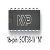
PCF8573P NXP Semiconductors, PCF8573P Datasheet - Page 8

PCF8573P
Manufacturer Part Number
PCF8573P
Description
Manufacturer
NXP Semiconductors
Datasheet
1.PCF8573P.pdf
(28 pages)
Specifications of PCF8573P
Time Format
HH:MM:SS
Package Type
PDIP
Operating Temperature Classification
Industrial
Operating Temperature (max)
85C
Operating Temperature (min)
-40C
Pin Count
16
Mounting
Through Hole
Lead Free Status / Rohs Status
Compliant
Available stocks
Company
Part Number
Manufacturer
Quantity
Price
Company:
Part Number:
PCF8573P
Manufacturer:
TI
Quantity:
12 948
Part Number:
PCF8573P
Manufacturer:
PHILIPS/飞利浦
Quantity:
20 000
Philips Semiconductors
8.3
Refer to Fig.6. A device generating a message is a ‘transmitter’, a device receiving a message is the ‘receiver’. The
device that controls the message is the ‘master’ and the devices which are controlled by the master are the ‘slaves’.
8.4
See Fig.7. The number of data bytes transferred between
the start and stop conditions from transmitter to receiver is
unlimited. Each byte of eight bits is followed by an
acknowledge bit. The acknowledge bit is a HIGH level
signal put on the bus by the transmitter during which time
the master generates an extra acknowledge related clock
pulse. A slave receiver which is addressed must generate
an acknowledge after the reception of each byte. Also a
master receiver must generate an acknowledge after the
reception of each byte that has been clocked out of the
slave transmitter.
2003 Jan 27
handbook, full pagewidth
Clock/calendar with serial I/O
System configuration
Acknowledge
SDA
SCL
BY TRANSMITTER
TRANSMITTER /
DATA OUTPUT
RECEIVER
DATA OUTPUT
BY RECEIVER
MASTER
SCL FROM
MASTER
condition
START
S
RECEIVER
Fig.7 Acknowledgment on the I
SLAVE
Fig.6 System configuration.
1
TRANSMITTER /
RECEIVER
SLAVE
8
The device that acknowledges must pull down the SDA
line during the acknowledge clock pulse, so that the SDA
line is stable LOW during the HIGH period of the
acknowledge related clock pulse (set-up and hold times
must be taken into consideration). A master receiver must
signal an end of data to the transmitter by not generating
an acknowledge on the last byte that has been clocked
out of the slave. In this event the transmitter must leave the
data line HIGH to enable the master to generate a stop
condition, see Figs. 10 and 11.
2
2
C-bus.
TRANSMITTER
not acknowledge
MASTER
acknowledge
8
acknowledgement
clock pulse for
9
TRANSMITTER /
RECEIVER
MBC602
MASTER
Product specification
PCF8573
MBA605


