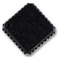
ADL5243ACPZ-R7 Analog Devices Inc, ADL5243ACPZ-R7 Datasheet - Page 26

ADL5243ACPZ-R7
Manufacturer Part Number
ADL5243ACPZ-R7
Description
IC RF FILTER VGA 32-LFCSP
Manufacturer
Analog Devices Inc
Series
-r
Specifications of ADL5243ACPZ-R7
Current - Supply
89mA
Frequency
100MHz ~ 4GHz
Gain
13dB
Noise Figure
3.7dB
P1db
26dBm
Package / Case
*
Rf Type
General Purpose
Test Frequency
2.63GHz
Voltage - Supply
4.75 V ~ 5.25 V
Frequency Range
0.1GHz To 4GHz
Noise Figure Typ
2.9dB
Power Dissipation Pd
1W
Supply Current
175mA
Supply Voltage Range
4.75V To 5.25V
Rohs Compliant
Yes
Number Of Channels
2
Frequency (max)
4GHz
Operating Supply Voltage (min)
4.75V
Operating Supply Voltage (typ)
5V
Operating Supply Voltage (max)
5.25V
Package Type
LFCSP EP
Mounting
Surface Mount
Pin Count
32
Operating Temp Range
-40C to 85C
Operating Temperature Classification
Industrial
Lead Free Status / Rohs Status
Lead free / RoHS Compliant
Other names
ADL5243ACPZ-R7TR
ADL5243
ADL5243
The typical configuration of the
AMP1-DSA-AMP2 mode, as shown in Figure 63. Because
AMP1and DSA are broadband in nature and internally
matched, only an ac-coupling capacitor is required between
them. The AMP2 is externally matched for each frequency band
of operation, and these matching elements should be placed
between the DSA and AMP2 and at the output of AMP2.
Figure 37 to Figure 45 show the performance of the
when connected in a loop for the three primary frequency
bands of operation, namely 943 MHz, 2140 MHz, and
2630 MHz.
RFIN
THERMAL CONSIDERATIONS
The
32-lead LFCSP. The thermal resistance from junction to air (θ
is 34.8°C/W. The thermal resistance for the product was
extracted assuming a standard 4-layer JEDEC board with 25
copper platter thermal vias. The thermal vias are filled with
conductive copper paste, AE3030, with a thermal conductivity
of 7.8 W/mk and thermal expansion as follows: α1 of 4 × 10
and α2 of 8.6 × 10
case (θ
frame package.
ADL5243
ADL5243
JC
) is 6.2°C/W, where case is the exposed pad of the lead
AMP1
LOOP PERFORMANCE
is packaged in a thermally efficient, 5 mm × 5 mm,
Figure 63.
VCC
−5
/°C. The thermal resistance from junction to
ADL5243
VDD/SPI
DSA
Loop Block Diagram
ADL5243
IMN
AMP2
is to connect in
VCC2
OMN
ADL5243
RFOUT
−5
Rev. A | Page 26 of 32
/°C
JA
)
For the best thermal performance, it is recommended to add as
many thermal vias as possible under the exposed pad of the
LFCSP. The above thermal resistance numbers assume a
minimum of 25 thermal vias arranged in a 5 × 5 array with a via
diameter of 13 mils, via pad of 25 mils, and pitch of 25 mils. The
vias are plated with copper, and the drill hole is filled with a
conductive copper paste. For optimal performance, it is
recommended to fill the thermal vias with a conductive paste of
equivalent thermal conductivity, as mentioned above, or use an
external heat sink to dissipate the heat quickly without affecting
the die junction temperature. It is also recommended to extend
the ground pattern as shown in Figure 64 to improve thermal
efficiency.
SOLDERING INFORMATION AND RECOMMENDED
PCB LAND PATTERN
Figure 64 shows the recommended land pattern for the ADL5243.
To minimize thermal impedance, the exposed paddle on the
5 mm × 5 mm LFCSP package is soldered down to a ground
plane. To improve thermal dissipation, 25 thermal vias are
arranged in a 5 × 5 array under the exposed paddle. If multiple
ground layers exist, they should be tied together using vias. For
more information on land pattern design and layout, see the
AN-772 Application Note, A Design and Manufacturing Guide for
the Lead Frame Chip Scale Package (LFCSP).
25 MIL VIA PAD
WITH 13 MIL VIA
Figure 64. Recommended Land Pattern
DSAIN
1
8
Data Sheet
24
DSAOUT
17


