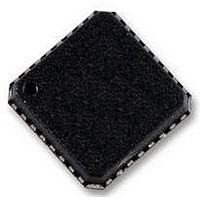
ADL5243ACPZ-R7 Analog Devices Inc, ADL5243ACPZ-R7 Datasheet - Page 10

ADL5243ACPZ-R7
Manufacturer Part Number
ADL5243ACPZ-R7
Description
IC RF FILTER VGA 32-LFCSP
Manufacturer
Analog Devices Inc
Series
-r
Specifications of ADL5243ACPZ-R7
Current - Supply
89mA
Frequency
100MHz ~ 4GHz
Gain
13dB
Noise Figure
3.7dB
P1db
26dBm
Package / Case
*
Rf Type
General Purpose
Test Frequency
2.63GHz
Voltage - Supply
4.75 V ~ 5.25 V
Frequency Range
0.1GHz To 4GHz
Noise Figure Typ
2.9dB
Power Dissipation Pd
1W
Supply Current
175mA
Supply Voltage Range
4.75V To 5.25V
Rohs Compliant
Yes
Number Of Channels
2
Frequency (max)
4GHz
Operating Supply Voltage (min)
4.75V
Operating Supply Voltage (typ)
5V
Operating Supply Voltage (max)
5.25V
Package Type
LFCSP EP
Mounting
Surface Mount
Pin Count
32
Operating Temp Range
-40C to 85C
Operating Temperature Classification
Industrial
Lead Free Status / Rohs Status
Lead free / RoHS Compliant
Other names
ADL5243ACPZ-R7TR
ADL5243
PIN CONFIGURATION AND FUNCTION DESCRIPTIONS
Table 3. Pin Function Descriptions
Pin No.
1, 24
2, 3, 5, 7, 8, 9, 11, 12, 13, 14,
17, 18, 20, 22, 23
4
6
10
15
16
19
21
25
26
27
28
29
30
31
32
Mnemonic
VDD
NC
DSAIN
AMP1OUT/VCC
AMP1IN
AMP2OUT/VCC2
VBIAS
AMP2IN
DSAOUT
D6
D5
D4
D3
D2/LE
D1/DATA
D0/CLK
SEL
EPAD
AMP1OUT/VCC
NOTES
1. NC = NO CONNECT. DO NOT CONNECT TO THIS PIN.
2. THE EXPOSED PAD MUST BE CONNECTED TO GROUND.
DSAIN
VDD
NC
NC
NC
NC
NC
Description
Supply Voltage for DSA. Connect this pin to a 5 V supply.
No Connect. Do not connect to this pin.
RF Input to DSA.
RF Output from Amplifier 1/Supply Voltage for Amplifier 1. Bias to Gain Block
Amplifier 1 is provided through a choke to this pin when connected to VCC.
RF Input to Gain Block Amplifier 1.
RF Output from Amplifier 2/Supply Voltage for Amplifier 2. Bias to Driver Amplifier 2 is
provided through a choke to this pin when connected to VCC2.
Bias for Driver Amplifier 2.
RF Input to Amplifier 2.
RF Output from DSA.
Data Bit in Parallel Mode (LSB). Connect to supply in serial mode.
Data Bit in Parallel Mode. Connect to ground in serial mode.
Data Bit in Parallel Mode. Connect to ground in serial mode.
Data Bit in Parallel Mode. Connect to ground in serial mode.
Data Bit in Parallel Mode/Latch Enable in Serial Mode.
Data Bit in Parallel Mode (MSB)/Data in Serial Mode.
Connect this pin to ground in parallel mode. This pin functions as a clock in serial
mode.
Select Pin. Connect this pin to the supply for parallel mode operation; connect this pin
to ground for serial mode operation.
Exposed Paddle. The exposed paddle must be connected to ground.
1
2
3
4
5
6
7
8
Figure 2. Pin Configuration
Rev. A | Page 10 of 32
(Not to Scale)
ADL5243
PIN 1
INDICATOR
TOP VIEW
24 VDD
23 NC
22 NC
21 DSAOUT
20 NC
19 AMP2IN
18 NC
17 NC
Data Sheet


