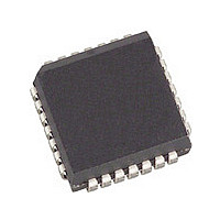
CY7B933-JCT Cypress Semiconductor Corp, CY7B933-JCT Datasheet - Page 27

CY7B933-JCT
Manufacturer Part Number
CY7B933-JCT
Description
Manufacturer
Cypress Semiconductor Corp
Datasheet
1.CY7B933-JCT.pdf
(33 pages)
Specifications of CY7B933-JCT
Lead Free Status / Rohs Status
Not Compliant
Available stocks
Company
Part Number
Manufacturer
Quantity
Price
Company:
Part Number:
CY7B933-JCT
Manufacturer:
NVIDIA
Quantity:
6 000
Document #: 38-02017 Rev. *E
CY7B923/CY7B933 Electrical Characteristics
Capacitance
AC Test Loads and Waveforms
Notes:
11. Maximum I
12. Maximum I
13. Tested initially and after any design or process changes that may affect these parameters, but not 100% tested.
14. Cypress uses constant current (ATE) load configurations and forcing functions. This figure is for reference only.
I
I
Parameter
C
CCT
CCR
Miscellaneous
IN
= 5.0V, T
V
V
unloaded. I
currents for each output pin. The total buffer quiescent current is 10mA max., and max. TTL load current for each output pin can be calculated as follows: Where R
load resistance, C
and temperature condition.
GND
CCN
CCN
3.0V
[11]
[12]
Parameter
R1 = 910Ω
R2 = 510Ω
C
(Includes fixture and
probe capacitance)
is determined by PECL load currents, typically 30 mA with 50 ohms to V
as described. When calculating the contribution of PECL load currents to chip power dissipation, the output load current should be multiplied by 1V instead of V
< 1 ns
L
A
< 30 pF
= 25°C, one output pair loaded with 50 ohms to V
CCR
CCT
CCR
Transmitter Power Supply
Current
Receiver Power Supply
Current
includes current into V
is measured with V
is measured with V
[13]
L
= capacitive load, and F
(c) TTL Input Test Waveform
1.0V
OUTPUT
2.0V
Input Capacitance
Description
CC
CC
(a) TTL AC Test Load
CCQ
= Max., one PECL output pair loaded with 50 ohms to V
= Max., RF = LOW, and outputs unloaded. Typical I
3.0V
(pins 21 and 24). Current into V
C
Description
L
TTLPin
I I CCN
pin
= frequency in MHz of data on pin. A derating factor of 1.1 has been included to account for worst process corner
=
5V
[
0.95 + (V CCN - 5) * 0.3
CC
2.0V
− 2.0V, others tied to V
Freq. = Max.
Freq. = Max.
R1
R2
1.0V
< 1 ns
R L
[14]
CCN
CC
T
(pin 9) is determined by the total TTL output buffer quiescent current plus the sum of all the load
A
Over the Operating Range
− 2.0V. Each additional enabled PECL pair adds 5 mA to I
+ C L * [
Test Conditions
= 25°C, f
Com’l
Ind’l and Mil
Com’l
Ind’l and Mil
CC
, BISTEN = LOW. I
V
V
CCR
IHE
ILE
V CCN
2
0
< 1 ns
(b) PECL AC Test Load
CC
is measured with V
Test Conditions
C
= 1 MHz, V
+ 1.5 ] * F pin
L
− 2.0V, and other PECL outputs tied to V
20%
CCT
(d) PECL Input Test Waveform
CC
]
includes current into V
* 1.1
CC
= 5.0V
80%
R
= 5.0V, T
[7]
L
(continued)
A
V
= 25°C, RF = LOW, BISTEN = LOW, and outputs
V
V
CC
[14]
IHE
ILE
Min.
Typ.
120
135
– 2
65
75
CCQ
80%
CC
(pin 9 and pin 22) only. Current into
CCT
R
C
(Includes fixture and
probe capacitance)
. Typical I
L
L
and an additional load current to
Max.
= 50 Ω
< 5 pF
10
CCT
Max.
Max.
CY7B923
CY7B933
20%
155
160
85
95
is measured with V
< 1 ns
Page 27 of 33
L
= equivalent
Unit
CC
pF
.
Unit
mA
mA
mA
mA
CC
[+] Feedback


