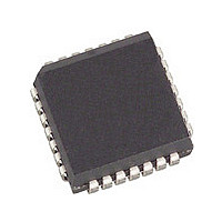
CY7B933-JCT Cypress Semiconductor Corp, CY7B933-JCT Datasheet - Page 10

CY7B933-JCT
Manufacturer Part Number
CY7B933-JCT
Description
Manufacturer
Cypress Semiconductor Corp
Datasheet
1.CY7B933-JCT.pdf
(33 pages)
Specifications of CY7B933-JCT
Lead Free Status / Rohs Status
Not Compliant
Available stocks
Company
Part Number
Manufacturer
Quantity
Price
Company:
Part Number:
CY7B933-JCT
Manufacturer:
NVIDIA
Quantity:
6 000
Document #: 38-02017 Rev. *E
safety functions), the FOTO input can be asserted. While it is
possible to insure that the output state of the PECL drivers is
LOW (i.e., light is off) by sending all 0’s in Bypass mode, it is
often inconvenient to insert this level of control into the data
transmission channel, and it is impossible in Encoded mode.
FOTO is provided to simplify and augment this control function
(typically found in laser-based transmission systems). FOTO
will force OUTA+ and OUTB+ to go LOW, OUTA– and OUTB–
to go HIGH, while allowing OUTC± to continue to function
normally (OUTC is typically used as a diagnostic feedback and
cannot be disabled). This separation of function allows various
system configurations without undue load on the control
function or data channel logic.
Transmitter Serial Data Characteristics
The CY7B923 HOTLink Transmitter serial output conforms to
the requirements of the Fibre Channel specification. The serial
data output is controlled by an internal Phase-Locked Loop
Control
Config
Status
Control
Config
Status
Data
Data
and
and
25
24
23
19
18
17
16
15
14
13
12
11
10
21
7
5
8
26
25
4
23
3
5
7
19
18
17
16
15
14
13
12
11
10
22
MODE
FOTO
BISTEN
ENN
ENA
RP
SC/D
D0
D1
D2
D3
D4
D5
D6
D7
SVS
MODE
BISTEN
SO
A/B
RF
RDY
SC/D
D0
D1
D2
D3
D4
D5
D6
D7
RVS
CKW
REFCLK
CKR
(Db)
(Dc)
(Dd)
(De)
(Di)
(Df)
(Dg)
(Dh)
(Qb)
(Qc)
(Qd)
(Qe)
(Qi)
(Qf)
(Qg)
(Qh)
(Dj)
(Qj)
Transmitter
(Da)
(Qa)
CY7B923
GND
6
CY7B933
Receiver
8
OUTA+
OUTA–
OUTB+
OUTB–
OUTC+
OUTC–
GND
VCC
9
20
4
VCC
Figure 5. HOTLink Connection Diagram
6
21
9 22
IB+
IB–
IA+
IA–
20
24
27
26
28
28
27
1
3
2
2
1
0.01 µF
Unused Output Left
0.01 µF
Open or Wired to V
to Minimize Power Dissipation
Tx PECL Load
C
D
E
A
B
E
C
D
270
270
CC
that multiplies the frequency of CKW by ten (10) to maintain
the proper bit clock frequency. The jitter characteristics
(including both PLL and logic components) are shown below:
Transmitter Test Mode Description
The CY7B923 Transmitter offers two types of test mode
operation, BIST mode and Test mode. In a normal system
application, the Built-In Self-Test (BIST) mode can be used to
check the functionality of the Transmitter, the Receiver, and
the link connecting them. This mode is available with minimal
impact on user system logic, and can be used as part of the
normal system diagnostics. Typical connections and timing
are shown in Figure 6.
• Deterministic Jitter (D
• Random Jitter (R
0.01 µF
Transmission
Termination
measured while sending a continuous K28.5 (C5.0).
measured while sending a continuous K28.7 (C7.0).
Tx PECL Load
82
82
Line
0.01 µF
PECL Load
Fiber Optic
130
130
82
82
0.01 µF
RL/2
RL/2
A
B
j
) < 175 ps (peak-peak). Typically
649
130
130
270
j
) < 35 ps (peak-peak). Typically
270
Signal Det.
Optional
270
1500
0.01 µF
0.01 µF
SIG
RX+
RX–
TX+
TX–
Fiber
Fiber
VCC
GND
VCC
GND
TX
RX
CY7B923
CY7B933
Fiber Optic
Twisted Pair
Twisted Pair
Fiber Optic
Coax or
Coax or
Page 10 of 33
Tx
Rx
[+] Feedback


