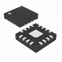
MAX4781ETE+T Maxim Integrated Products, MAX4781ETE+T Datasheet - Page 8

MAX4781ETE+T
Manufacturer Part Number
MAX4781ETE+T
Description
IC MULTIPLEXER 8X1 16TQFN
Manufacturer
Maxim Integrated Products
Datasheet
1.MAX4782ETET.pdf
(16 pages)
Specifications of MAX4781ETE+T
Function
Multiplexer
Circuit
1 x 8:1
On-state Resistance
1 Ohm
Voltage Supply Source
Single Supply
Voltage - Supply, Single/dual (±)
1.6 V ~ 3.6 V
Current - Supply
1µA
Operating Temperature
-40°C ~ 85°C
Mounting Type
Surface Mount
Package / Case
16-TQFN Exposed Pad
Lead Free Status / RoHS Status
Lead free / RoHS Compliant
Other names
MAX4781ETE+TTR
High-Speed, Low-Voltage, 0.7Ω CMOS Analog
Switches/Multiplexers
The MAX4781/MAX4782/MAX4783 construction is typical
of most CMOS analog switches. There are two supply
inputs: V
CMOS switches and set the limits of the analog voltage
on any switch. Internal reverse ESD-protection diodes are
connected between each analog signal input and both
V
GND, one of these diodes conducts. During normal oper-
ation, these and other reverse-biased ESD diodes leak,
forming the only current drawn from V
Virtually all the analog leakage current comes from the
ESD diodes. Although the ESD diodes on a given sig-
nal input are identical and therefore fairly well bal-
anced, they are reverse-biased differently. Each diode
is biased by either V
Their leakages vary as the signal varies. The difference
in the two diodes’ leakages to V
tutes the analog-signal-path leakage current. All analog
leakage current flows between each input and one of
the supply terminals, not to the other switch terminal.
Both sides of a given switch can show leakage currents
of either the same or opposite polarity.
V
logic limits. Logic inputs have ESD-protection diodes
to ground.
The MAX4781/MAX4782/MAX4783 operate from a sin-
gle supply between +1.6V and +3.6V. Switch on-resis-
tance increases as the supply voltage is lowered.
8
CC
CC
_______________________________________________________________________________________
and GND power the internal logic and set the input
and GND. If any analog signal exceeds V
CC
and GND. V
Applications Information
Power-Supply Considerations
CC
or GND and the analog signal.
CC
and GND drive the internal
CC
CC
and GND consti-
or GND.
Power Supply
Overview
CC
or
In 50Ω systems, signal response is reasonably flat up
to 50MHz (see the Typical Operating Characteristics).
Above 20MHz, the on-response has several minor
peaks that are highly layout dependent. In the off state,
the switch acts like a capacitor and passes higher fre-
quencies with less attenuation. At 10MHz, off-isolation
is approximately -50dB in 50Ω systems, becoming
worse (approximately 20dB per decade) as frequency
increases. Higher circuit impedance also degrades off-
isolation. Adjacent channel attenuation is approximate-
ly 3dB above that of a bare IC socket and is entirely
because of capacitive coupling.
The MAX4781/MAX4782/MAX4783 are pin compatible
with the industry-standard 74HC4051/74HC4052/
74HC4053 and the MAX4617/MAX4618/MAX4619. In
single-supply applications, they function identically and
have identical logic diagrams, although these parts dif-
fer electrically. The pin designations and logic dia-
grams in this data sheet conform to the original 1972
specifications published by RCA for the CD4051/
CD4052/CD4053. These designations differ from the
standard Maxim switch and mux designations found on
other Maxim data sheets such as the MAX4051/
MAX4052/MAX4053. Designers who are more comfort-
able with Maxim’s standard designations are advised
that the pin designations and logic diagrams on the
MAX4051/MAX4052/MAX4053 data sheet can be
applied to the MAX4781/MAX4782/MAX4783.
High-Frequency Performance
Pin Nomenclature


