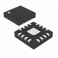
MAX4781ETE+T Maxim Integrated Products, MAX4781ETE+T Datasheet - Page 2

MAX4781ETE+T
Manufacturer Part Number
MAX4781ETE+T
Description
IC MULTIPLEXER 8X1 16TQFN
Manufacturer
Maxim Integrated Products
Datasheet
1.MAX4782ETET.pdf
(16 pages)
Specifications of MAX4781ETE+T
Function
Multiplexer
Circuit
1 x 8:1
On-state Resistance
1 Ohm
Voltage Supply Source
Single Supply
Voltage - Supply, Single/dual (±)
1.6 V ~ 3.6 V
Current - Supply
1µA
Operating Temperature
-40°C ~ 85°C
Mounting Type
Surface Mount
Package / Case
16-TQFN Exposed Pad
Lead Free Status / RoHS Status
Lead free / RoHS Compliant
Other names
MAX4781ETE+TTR
ABSOLUTE MAXIMUM RATINGS
Voltages Referenced to GND
Continuous Current into A, B, C, ENABLE........................±10mA
Continuous Current into X, Y, Z, X_, Y_, Z_ ....................±150mA
Peak Current into X, Y, Z, X_, Y_, Z_
High-Speed, Low-Voltage, 0.7Ω CMOS Analog
Switches/Multiplexers
ELECTRICAL CHARACTERISTICS—Single +3V Supply
(V
T
Note 1: Signals on X, Y, Z, X_, Y_, and Z_ exceeding V
Stresses beyond those listed under “Absolute Maximum Ratings” may cause permanent damage to the device. These are stress ratings only, and functional
operation of the device at these or any other conditions beyond those indicated in the operational sections of the specifications is not implied. Exposure to
absolute maximum rating conditions for extended periods may affect device reliability.
2
A
ANALOG SWITCH
Analog Signal Range
On-Resistance (Note 4)
On-Resistance Match
Between Channels
(Notes 4, 5)
On-Resistance Flatness
(Note 6)
X_, Y_, Z_
Off-Leakage Current
X Off-Leakage Current
(MAX4781 Only)
X On-Leakage Current
(MAX4781 Only)
X, Y, Z Off-Leakage Current
(MAX4782/MAX4783 Only)
X, Y, Z On-Leakage Current
(MAX4782/MAX4783 Only)
CC
V
Voltage at Any Other Terminal
(Note 1)...................................................-0.3V to (V
(pulsed at 1ms, 10% duty cycle)................................±300mA
= +25°C.) (Notes 2, 3)
CC
_______________________________________________________________________________________
= +2.7V to +3.6V, GND = 0, V
, A, B, C, and ENABLE ...............................-0.3V to +4.6V
maximum current rating.
PARAMETER
V
V
X
R
SYMBOL
_, V
X
I
I
I
FLAT(ON)
I
I
I
I
X_(OFF)
Y_(OFF)
Z_(OFF)
∆R
I
I
I
I
, V
X(OFF)
X(OFF)
Y(OFF)
Z(OFF)
X(ON)
X(ON)
Y(ON)
Z(ON)
R
IH
ON
Y
Y
ON
_, V
, V
= 1.4V, V
Z
Z
,
_
V
100m A; V
V
100m A; V
V
100m A; V
1.7V
V
V
V
V
V
V
V
V
V
V
V
V
V
V
V
C C
X_
X_
C C
C C
C C
C C
Y
C C
X_
X_
C C
X _
Y
C C
X
Z
X _
, V
, V
, V
= 0.3V, 3.3V or floating
IL
, V
CC
, V
= 0.3V , 3.3V ;
= 0.3V , 3.3V or fl oati ng
= 3.3V , 0.3V ;
= 0.3V, 3.3V
= +3.6V
= + 2.7V ; I
= + 2.7V ; I
= + 2.7V ; I
= + 3.6V ;
= + 3.6V ;
= + 3.6V ;
= + 3.6V ;
Z
Z
Y
Y_
= 0.5V, T
, V
Y_
= 0.3V, 3.3V
= 0.3V, 3.3V
+ 0.3V)
CONDITIONS
, V
, V
Z
CC
X
X
X
= 0.3V , 3.3V ; V
Z_
, V
, V
, V
Z_
or GND are clamped by internal diodes. Limit forward-diode current to
= 3.3V , 0.3V ; V
Y
Y
Y
= 3.3V , 0.3V ; V
X _
X _
X _
, V
, V
, V
, I
, I
, I
A
Z
Z
Z
Y _
Y _
Y _
= T
= 1.7V
= 1.7V
= 0, 0.7V,
, I
, I
, I
Continuous Power Dissipation
Operating Temperature Range ..........................-40°C to +85°C
Junction Temperature ......................................................+150°C
Storage Temperature Range .............................-65°C to +150°C
Lead Temperature (soldering, 10s) .................................+300°C
Z _
Z _
Z _
MIN
16-Pin Thin QFN (derate 16.9mW/°C above +70°C) ...1349mW
16-Pin TSSOP (derate 5.7mW/°C above +70°C) ........ 457mW
=
=
=
X
, V
X
to T
X
Y
,
,
,
MAX
+25°C
T
+25°C
T
+25°C
T
+25°C
T
+25°C
T
+25°C
T
+25°C
T
+25°C
T
MIN
MIN
MIN
MIN
MIN
MIN
MIN
MIN
, unless otherwise noted. Typical values are at
to T
to T
to T
to T
to T
to T
to T
to T
T
A
MAX
MAX
MAX
MAX
MAX
MAX
MAX
MAX
MIN
-50
-50
-25
-25
-2
-7
-2
-2
-2
-2
0
0.002
0.002
0.002
0.002
0.002
TYP
0.7
0.3
0.1
MAX
V
+50
+50
+25
+25
1.2
0.4
0.6
0.2
0.2
+2
+7
+2
+2
+2
+2
CC
1
UNITS
nA
nA
nA
nA
nA
Ω
Ω
Ω
V


