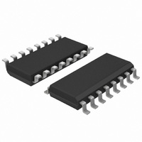
HEF4051BT,652 NXP Semiconductors, HEF4051BT,652 Datasheet - Page 6

HEF4051BT,652
Manufacturer Part Number
HEF4051BT,652
Description
IC MUX/DEMUX 8X1 16SOIC
Manufacturer
NXP Semiconductors
Series
4000Br
Type
Analog Multiplexerr
Datasheet
1.HEF4051BT653.pdf
(23 pages)
Specifications of HEF4051BT,652
Package / Case
16-SOIC (0.154", 3.90mm Width)
Function
Multiplexer/Demultiplexer
Circuit
1 x 8:1
On-state Resistance
175 Ohm
Voltage Supply Source
Single, Dual Supply
Voltage - Supply, Single/dual (±)
3 V ~ 15 V, ±15 V
Current - Supply
80µA
Operating Temperature
-40°C ~ 85°C
Mounting Type
Surface Mount
Number Of Channels
1 Channel
On Resistance (max)
2500 Ohm @ 5 V
On Time (max)
280 ns @ 5 V
Off Time (max)
290 ns @ 5 V
Supply Voltage (max)
15 V
Supply Voltage (min)
3 V
Maximum Operating Temperature
+ 85 C
Minimum Operating Temperature
- 40 C
Mounting Style
SMD/SMT
Number Of Switches
Single
Multiplexer Configuration
Single 8:1
Number Of Inputs
8
Number Of Outputs
1
Analog Switch On Resistance
2500@5VOhm
Package Type
SO
Power Supply Requirement
Single
Single Supply Voltage (min)
3V
Single Supply Voltage (typ)
5/9/12V
Single Supply Voltage (max)
15V
Dual Supply Voltage (min)
Not RequiredV
Dual Supply Voltage (typ)
Not RequiredV
Dual Supply Voltage (max)
Not RequiredV
Mounting
Surface Mount
Pin Count
16
Operating Temp Range
-40C to 85C
Operating Temperature Classification
Industrial
Lead Free Status / RoHS Status
Lead free / RoHS Compliant
Lead Free Status / RoHS Status
Lead free / RoHS Compliant, Lead free / RoHS Compliant
Other names
568-3979-5
933372940652
HEF4051BTD
HEF4051BTD
933372940652
HEF4051BTD
HEF4051BTD
NXP Semiconductors
7. Functional description
Table 3.
[1]
8. Limiting values
Table 4.
In accordance with the Absolute Maximum Rating System (IEC 60134). Voltages are referenced to V
[1]
[2]
HEF4051B_9
Product data sheet
Input
E
L
L
L
L
L
L
L
L
H
Symbol
V
V
I
V
I
I
T
T
P
P
IK
I/O
DD
stg
amb
DD
EE
I
tot
H = HIGH voltage level;
L = LOW voltage level;
X = don’t care.
To avoid drawing V
switch must not exceed 0.4 V. If the switch current flows into terminal Z, no V
is no limit for the voltage drop across the switch, but the voltages at Y and Z may not exceed V
For DIP16 package: P
Function table
Limiting values
Parameter
supply voltage
supply voltage
input clamping current
input voltage
input/output current
supply current
storage temperature
ambient temperature
total power dissipation
power dissipation
7.1 Function table
DD
current out of terminal Z, when switch current flows into terminals Y, the voltage drop across the bidirectional
tot
S3
L
L
L
L
H
H
H
H
X
derates linearly with 12 mW/K above 70 °C.
[1]
All information provided in this document is subject to legal disclaimers.
Conditions
referenced to V
pins Sn and E;
V
T
per output
amb
I
DIP16 package
SO16 package
SSOP16 package
TSSOP16 package
< −0.5 V or V
S2
L
L
H
H
L
L
H
H
X
Rev. 09 — 25 March 2010
= −40 °C to +125 °C
DD
I
> V
DD
+ 0.5 V
DD
8-channel analog multiplexer/demultiplexer
current will flow out of terminals Y, and in this case there
S1
L
H
L
H
L
H
L
H
X
[1]
[2]
Min
−0.5
−18
-
−0.5
-
-
−65
−40
-
-
-
-
-
DD
or V
EE
.
Max
+18
+0.5
±10
V
±10
+150
+125
750
500
500
500
100
50
HEF4051B
Channel ON
Y0 to Z
Y1 to Z
Y2 to Z
Y3 to Z
Y4 to Z
Y5 to Z
Y6 to Z
Y7 to Z
switches off
DD
SS
+ 0.5
= 0 V (ground).
© NXP B.V. 2010. All rights reserved.
Unit
V
V
mA
V
mA
mA
°C
°C
mW
mW
mW
mW
mW
6 of 23


