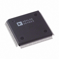
AD9887AKS-140 Analog Devices Inc, AD9887AKS-140 Datasheet - Page 8

AD9887AKS-140
Manufacturer Part Number
AD9887AKS-140
Description
IC INTRFACE ANALOG/DVI 160-MQFP
Manufacturer
Analog Devices Inc
Datasheet
1.AD9887AKSZ-100.pdf
(40 pages)
Specifications of AD9887AKS-140
Rohs Status
RoHS non-compliant
Applications
Graphic Cards, VGA Interfaces
Interface
Analog and Digital
Voltage - Supply
3.15 V ~ 3.45 V
Package / Case
160-MQFP, 160-PQFP
Mounting Type
Surface Mount
Available stocks
Company
Part Number
Manufacturer
Quantity
Price
Company:
Part Number:
AD9887AKS-140
Manufacturer:
AD
Quantity:
275
Company:
Part Number:
AD9887AKS-140
Manufacturer:
TOS
Quantity:
160
Company:
Part Number:
AD9887AKS-140
Manufacturer:
AD
Quantity:
586
Part Number:
AD9887AKS-140
Manufacturer:
ADI/亚德诺
Quantity:
20 000
AD9887
DESCRIPTIONS OF PINS SHARED BETWEEN ANALOG
AND DIGITAL INTERFACES
HSOUT
VSOUT
Serial Port (2-Wire)
SDA
SCL
A0
A1
Data Outputs
RED A
RED B
GREEN A
GREEN B
BLUE A
BLUE B
Horizontal Sync Output
A reconstructed and phase-aligned version of
the video HSYNC. The polarity of this output
can be controlled via a serial bus bit. In analog
interface mode the placement and duration
are variable. In digital interface mode the
placement and duration are set by the graphics
transmitter.
Vertical Sync Output
The separated VSYNC from a composite
signal or a direct pass through of the VSYNC
input. The polarity of this output can be con-
trolled via a serial bus bit. The placement and
duration in all modes is set by the graphics
transmitter.
Serial Port Data I/O
Serial Port Data Clock
Serial Port Address Input 1
Serial Port Address Input 2
For a full description of the 2-wire serial regis-
ter and how it works, refer to the Control
Register section.
Data Output, Red Channel, Port A/Even
Data Output, Red Channel, Port B/Odd
Data Output, Green Channel, Port A/Even
Data Output, Green Channel, Port B/Odd
Data Output, Blue Channel, Port A/Even
Data Output, Blue Channel, Port B/Odd
The main data outputs. Bit 7 is the MSB.
These outputs are shared between the two
interfaces and behave according to which
interface is active. Refer to the sections on the
two interfaces for more information on how
these outputs behave.
Data Clock Outputs
DATACK
DATACK
Various
S
SCAN Function
SCAN
SCAN
SCAN
CDT
IN
OUT
CLK
Data Output Clock
Data Output Clock Complement
Just like the data outputs, the data clock out-
puts are shared between the two interfaces.
They also behave differently depending on
which interface is active. Refer to the sections
on the two interfaces to determine how these
pins behave.
Chip Active/Inactive Detect Output
The logic for the S
HSYNC detection] OR [digital interface DE
detection]. So, the S
logic LOW under two conditions, when nei-
ther interface is active or when the chip is in
full chip power-down mode. The data outputs
are automatically three-stated when S
LOW. This pin can be read by a controller in
order to determine periods of inactivity.
Data Input for SCAN Function
Data can be loaded serially into the 48-bit
SCAN register through this pin, clocking it in
with the SCAN
the 48 data outputs in parallel. This function
is useful for loading known data into a graph-
ics controller chip for testing purposes.
Data Output for SCAN Function
The data in the 48-bit SCAN register can be
read through this pin. Data is read on a FIFO
basis and is clocked via the SCAN
Data Clock for SCAN Function
This pin clocks the data through the SCAN
register. It controls both data input and data
output.
CLK
CDT
pin. It then comes out of
CDT
pin is [analog interface
pin will switch to
CLK
CDT
pin.
is


