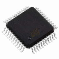
PSD303B-70M STMicroelectronics, PSD303B-70M Datasheet - Page 36

PSD303B-70M
Manufacturer Part Number
PSD303B-70M
Description
MCU 8BIT PROGRM 70NS 44-PQFP
Manufacturer
STMicroelectronics
Datasheet
1.PSD303B-70M.pdf
(85 pages)
Specifications of PSD303B-70M
Applications
*
Interface
*
Voltage - Supply
*
Package / Case
44-MQFP, 44-PQFP
Mounting Type
Surface Mount
Lead Free Status / RoHS Status
Lead free / RoHS Compliant
Available stocks
Company
Part Number
Manufacturer
Quantity
Price
Company:
Part Number:
PSD303B-70M
Manufacturer:
STMicroelectronics
Quantity:
10 000
16.0
Power
Management
(cont.)
All the inputs shown, except CSI, go to the PAD logic. These signals must be taken into
consideration when calculating the composite frequency. Before we make the calculation,
let’s establish the following conditions:
Now, lets assume the following is a snapshot in time of all the input signals during a typical
80C31 bus cycle. We’ll use a code fetch as an example since that happens most often.
The calculation of the composite frequency is as follows:
16.6 Loading on I/O pins
A final consideration when calculating the current usage for the entire PSD device is the
loading on I/O pins. All specifications for PSD current consumption in this document
assume zero current flowing through PSD I/O pins (including ADIO). I/O current is dictated
by the individual design implementation, and must be calculated by the designer. Be aware
that I/O current is a function of loading on the pins and the frequency at which the signals
toggle.
•
•
•
•
•
•
•
•
•
The input with the highest frequency is ALE, which is 2 MHz. So our base period is
500 nsec for this example.
Only the address information from the multiplexed signals AD0-AD7 reach the PAD
logic because of the internal address latch. Signal transitions from data on AD0-AD7
do not reach the PADs.
The three inputs (Int, Sel, or Rdy) change state very infrequently relative to the 80C31
bus signals.
There are four distinct transitions (first four dotted lines) within the base period of
500 nsec. These first four transitions all count toward the final composite frequency.
The transition at (1) in the diagram does not count as a distinct transition because it is
within 25 nsec of a neighboring transition (use 50 nsec for a ZPSD3XXV device).
Transition (2) above does not add to the composite frequency because only the
internally latched address signals reach the PADs, the data signal transitions do not.
The transition at (3) just happens to appear in this snapshot, but its frequency is so
low that it is not a significant contributor to the overall composite frequency, and will
not be used.
Divide the 500 nsec base period by the four (distinct transitions), yielding 125 nsec.
1/125 nsec = 8 MHz.
Use 8 MHz as the composite frequency of PAD inputs when calculating current
consumption. (See the next section for a sample current calculation.)
AD0-AD7
A8-A15
PSEN
RDY
ALE
SEL
INT
ONE TYPICAL 80C31 BUS CYCLE (2 MHz, 500 nsec)
FOUR DISTINCT
TRANSITIONS
ADDR
1
< 25 nsec
2
DATA
3
PSD3XX Family
33


