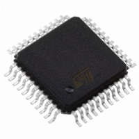
PSD303B-70M STMicroelectronics, PSD303B-70M Datasheet - Page 11

PSD303B-70M
Manufacturer Part Number
PSD303B-70M
Description
MCU 8BIT PROGRM 70NS 44-PQFP
Manufacturer
STMicroelectronics
Datasheet
1.PSD303B-70M.pdf
(85 pages)
Specifications of PSD303B-70M
Applications
*
Interface
*
Voltage - Supply
*
Package / Case
44-MQFP, 44-PQFP
Mounting Type
Surface Mount
Lead Free Status / RoHS Status
Lead free / RoHS Compliant
Available stocks
Company
Part Number
Manufacturer
Quantity
Price
Company:
Part Number:
PSD303B-70M
Manufacturer:
STMicroelectronics
Quantity:
10 000
Table 2.
PSD3XX Pin
Descriptions
8
PSD3XX Family
Legend:
RD/E/DS
R/W/V
A19/CSI
WR/V
ALE/AS
Name
PSEN
Reset
BHE/
PA0
PA1
PA2
PA3
PA4
PA5
PA6
PA7
or
PP
PP
The Type column abbreviations are: I = input only; I/O = input/output; P = power.
Type
I/O
I
I
I
I
I
I
When the data bus is 8 bits:
This pin is for 8031 or compatible MCUs that use PSEN to
separate program space from data space. In this case, PSEN is
used for reads from the EPROM. Note: if your MCU does not
output a PSEN signal, pull up this pin to V
When the data bus is 16 bits:
This pin is BHE. When low, D8-D15 are read from or written to.
Note: in programming mode, this pin is pulsed between V
The following control signals can be connected to this port, based on
your MCU (and the way you configure the PSD in PSDsoft):
1. WR—active-low write pulse.
2. R/W—active-high read/active-low write input.
Note: in programming mode, this pin must be tied to V
The following control signals can be connected to this port, based on
your MCU (and the way you configure the PSD in PSDsoft):
1. RD—active-low read input.
2. E—E clock input.
3. DS—active-low data strobe input (3X2/3X3 devices only)
The following control signals can be connected to this port:
1. CSI—Active-low chip select input. If your MCU supports a chip
2. If you don’t wish to use the CSI feature, you may use this pin as
PSD3XX/ZPSD3XX:
This pin is user-programmable and can be configured to reset on a
high- or low-level input. Reset must be applied for at least 100 ns.
ZPSD3XXV:
This pin is not configurable, and the chip will only reset on an
active-low level input. Reset must be applied for at least 500 ns,
and no operations may take place for an additional 500 ns minimum.
(See Figure 8.)
If you use an MCU that has a multiplexed bus:
Connect ALE or AS to this pin. The polarity of this pin is configurable.
The trailing edge of ALE/AS latches all multiplexed address inputs
(and BHE where applicable).
If you use an MCU that does not have a multiplexed bus:
If your MCU uses ALE/AS, connect the signal to this pin.
Otherwise, use this pin for a generic logic input to the PAD.
(Non-3X1 devices only.)
These pins make up Port A. These port pins are configurable, and
can have the following functions: (see Figure 5A and 5B)
1. Track AD7-AD0. This feature repeats the MCU address and data
2. MCU I/O—in this mode, the direction of the pin is defined by its
3. Latched address output.
4. CMOS or open-drain output.
5. If your MCU is non-multiplexed: data bus input—connect your
bus on all Port A pins.
direction bit, which resides in the direction register.
data bus (D0-7) to these pins. See Figure 3.
select output, and you want the PSD to save power when not
selected, use this pin as a chip select input.
an additional input (logic or address) to the PAD. A19 can be
latched (with ALE/AS), or a transparent logic input.
Description
CC
.
PP
PP
.
and 0 V.


