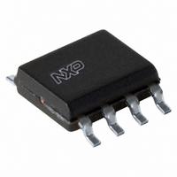
PCA9600D,112 NXP Semiconductors, PCA9600D,112 Datasheet - Page 5

PCA9600D,112
Manufacturer Part Number
PCA9600D,112
Description
IC DUAL BI-DIR BUS BUFFER 8-SOIC
Manufacturer
NXP Semiconductors
Type
Bufferr
Datasheet
1.PCA9600D112.pdf
(31 pages)
Specifications of PCA9600D,112
Package / Case
8-SOIC (3.9mm Width)
Mounting Type
Surface Mount
Current - Supply
7.3mA
Voltage - Supply
2.5 V ~ 15 V
Delay Time
100ns
Capacitance - Input
10pF
Tx/rx Type
I²C Logic
Supply Voltage (max)
15 V
Supply Voltage (min)
2.5 V
Maximum Operating Temperature
+ 85 C
Mounting Style
SMD/SMT
Minimum Operating Temperature
- 40 C
Lead Free Status / RoHS Status
Lead free / RoHS Compliant
Other names
935285243112::PCA9600D::PCA9600D
NXP Semiconductors
Table 4.
PCA9600
Product data sheet
Detail
Supply voltage (V
Maximum operating bus voltage
(independent of V
Typical operating supply current:
Typical LOW-level input voltage on I
(SX/SY side):
LOW-level output voltage on I
(SX/SY side; 3 mA sink):
LOW-level output voltage on Fm+ I
(SX/SY side; 7 mA sink):
Temperature coefficient of V
Logic voltage levels on SX/SY bus
(independent of V
Typical propagation delays:
TX/RX switching specifications (I
compliant):
RX logic levels with tighter control than
I
Maximum bus speed:
ESD rating HBM per JESD22-A114:
Package:
2
C-bus limit of 30 % to 70 %:
PCA9600 versus P82B96
CC
CC
CC
) range:
):
):
Remark: Two or more SX or SY I/Os must not be interconnected. The PCA9600 design
does not support this configuration. Bidirectional I
direction control pin so, instead, slightly different logic LOW voltage levels are used at
SX/SY to avoid latching of this buffer. A ‘regular I
PCA9600 will be propagated to SX/SY as a ‘buffered LOW’ with a slightly higher voltage
level. If this special ‘buffered LOW’ is applied to the SX/SY of another PCA9600, that
second PCA9600 will not recognize it as a ‘regular I
to its TX/TY output. The SX/SY side of PCA9600 may not be connected to similar buffers
that rely on special logic thresholds for their operation, for example P82B96, PCA9511A,
PCA9515A, ‘B’ side of PCA9517, etc. The SX/SY side is only intended for, and compatible
with, the normal I
TX/RX signals of a second PCA9600 or P82B96 if required. The TX/RX and TY/RY I/O
pins use the standard I
restrictions on the interconnection of the TX/RX and TY/RY I/O pins to other PCA9600s,
for example in a star or multipoint configuration with the TX/RX and TY/RY I/O pins on the
common bus and the SX/SY side connected to the line card slave devices. For more
details see Application Note AN10658, “Sending I
cables”.
The PCA9600 is a direct upgrade of the P82B96 with the significant differences
summarized in
IL
2
/ V
C-bus
2
OL
C-bus
2
:
C-bus
2
C-bus
Table
All information provided in this document is subject to legal disclaimers.
2
C-bus logic voltage levels of I
PCA9600
2.5 V to 15 V
15 V
5 mA
0.5 V over −40 °C to +85 °C
0.74 V (max.) over −40 °C to +85 °C
1 V (max.)
0 mV/°C
compatible with I
buses using TTL levels (SMBus, etc.)
< 100 ns
yes, all classes including 1 MHz Fm+ yes, all classes including Fm+
yes, 40 % to 55 % (48 % nominal)
> 1 MHz
> 4500 V
SO8, TSSOP8 (MSOP8)
4.
2
C-bus logic voltage levels of all I
Rev. 5 — 5 May 2011
2
C-bus and similar
2
C-bus master and slave chips, or even
2
2
2
C-bus LOW’ applied at the RX/RY of a
C-bus signals do not allow any
C-bus signals via long communication
2
C-bus LOW’ and will not propagate it
2 V to 15 V
n/a
< 200 ns
yes, 42 % to 58 % (50 % nominal)
> 400 kHz
P82B96
15 V
1 mA
0.65 V at 25 °C
0.88 V (typ.) at 25 °C
−2 mV/°C
compatible with I
buses using TTL levels (SMBus, etc.)
> 3500 V
DIP8, SO8, TSSOP8 (MSOP8)
2
C-bus parts. There are no
Dual bidirectional bus buffer
PCA9600
2
C-bus and similar
© NXP B.V. 2011. All rights reserved.
5 of 31


