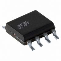
PCA9600D,112 NXP Semiconductors, PCA9600D,112 Datasheet - Page 19

PCA9600D,112
Manufacturer Part Number
PCA9600D,112
Description
IC DUAL BI-DIR BUS BUFFER 8-SOIC
Manufacturer
NXP Semiconductors
Type
Bufferr
Datasheet
1.PCA9600D112.pdf
(31 pages)
Specifications of PCA9600D,112
Package / Case
8-SOIC (3.9mm Width)
Mounting Type
Surface Mount
Current - Supply
7.3mA
Voltage - Supply
2.5 V ~ 15 V
Delay Time
100ns
Capacitance - Input
10pF
Tx/rx Type
I²C Logic
Supply Voltage (max)
15 V
Supply Voltage (min)
2.5 V
Maximum Operating Temperature
+ 85 C
Mounting Style
SMD/SMT
Minimum Operating Temperature
- 40 C
Lead Free Status / RoHS Status
Lead free / RoHS Compliant
Other names
935285243112::PCA9600D::PCA9600D
NXP Semiconductors
PCA9600
Product data sheet
testing but it was not damaged. Whenever there is current flowing in any of these diodes it
is possible that there can be faulty operation of any IC. For that reason we put a
specification on the negative voltage that is allowed to be applied. It is selected so that, at
the highest allowed junction temperature, there will be a big safety factor that guarantees
the diode will not conduct and then we do not need to make any 100 % production tests to
guarantee the published specification.
For the PCA9600, in specific applications, there will always be transient overshoot and
ringing on the wiring that can cause these diodes to conduct. Therefore we designed the
IC to withstand those transients and as a part of the qualification procedure we made
tests, using DC currents to more than twice the normal bus sink currents, to be sure that
the IC was not affected by those currents. For example, the TX/TY and RX/RY pins were
tested to at least −80 mA which, from
functioning of the PCA9600 is not affected even by those large currents. The Absolute
Maximum (DC) ratings are not intended to apply to transients but to steady state
conditions. This explains why you will never see any problems in practice even if, during
transients, more than −0.3 V is applied to the bus interface pins of PCA9600.
Figure 22 “Diode characteristic curve”
DC specification was selected. The current at 25 °C is near zero at −0.55 V. The
PCA9600 is allowed to operate with +125 °C junction and that would cause this diode
voltage to decrease by 100 × 2 mV = 200 mV. So for zero current we need to specify
−0.35 V and we publish −0.3 V just to have some extra margin.
Remark: You should not be concerned about the transients generated on the wiring by a
PCA9600 in normal applications and that is input to the TX/RX or TY/RY pins of another
PCA9600. Because not all ICs that may be driven by PCA9600 are designed to tolerate
negative transients, in
they can be managed if required.
Fig 22. Diode characteristic curve
All information provided in this document is subject to legal disclaimers.
diode current
−10
(mA)
−10
−10
−10
Section 10.2.1 “Example with questions and answers”
−10
−1
−1
Rev. 5 — 5 May 2011
0
2
3
4
−2.0
−1.5
Figure
also explains how the general Absolute Maximum
−1.0
22, would be more than −0.8 V. The correct
−0.5
voltage (V)
002aaf063
Dual bidirectional bus buffer
0
PCA9600
© NXP B.V. 2011. All rights reserved.
we show
19 of 31


