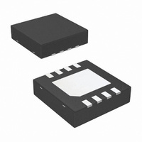
DS25BR150TSD/NOPB National Semiconductor, DS25BR150TSD/NOPB Datasheet - Page 5

DS25BR150TSD/NOPB
Manufacturer Part Number
DS25BR150TSD/NOPB
Description
IC BUFFER/REPEATER LVDS 8-LLP
Manufacturer
National Semiconductor
Type
Bufferr
Datasheet
1.DS25BR150TSDNOPB.pdf
(12 pages)
Specifications of DS25BR150TSD/NOPB
Tx/rx Type
LVDS
Delay Time
465ps
Capacitance - Input
1.7pF
Voltage - Supply
3 V ~ 3.6 V
Current - Supply
43mA
Mounting Type
Surface Mount
Package / Case
8-LLP
Supply Current
35mA
Supply Voltage Range
3V To 3.6V
Driver Case Style
LLP
No. Of Pins
8
Operating Temperature Range
-40°C To +85°C
Msl
MSL 3 - 168 Hours
Filter Terminals
SMD
Logic Type
Buffer
Rohs Compliant
Yes
Data Rate
3.125Gbps
Data Rate Max
3.125Gbps
For Use With
DS25BR150EVK - BOARD EVALUATION DS25BR150
Lead Free Status / RoHS Status
Lead free / RoHS Compliant
Other names
DS25BR150TSD
DS25BR150TSDTR
DS25BR150TSDTR
Available stocks
Company
Part Number
Manufacturer
Quantity
Price
Company:
Part Number:
DS25BR150TSD/NOPB
Manufacturer:
NXP
Quantity:
4 930
LVDS OUTPUT AC SPECIFICATIONS (OUT+, OUT-)
t
t
t
t
t
t
JITTER PERFORMANCE (Figure 5)
t
t
t
t
t
t
Symbol
PHLD
PLHD
SKD1
SKD2
LHT
HLT
DJ1
DJ2
RJ1
RJ2
TJ1
TJ2
AC Electrical Characteristics
Over recommended operating supply and temperature ranges unless otherwise specified. (Notes 9, 10)
Note 9: The Electrical Characteristics tables list guaranteed specifications under the listed Recommended Operating Conditions except as otherwise modified
or specified by the Electrical Characteristics Conditions and/or Notes. Typical specifications are estimations only and are not guaranteed.
Note 10: Typical values represent most likely parametric norms for V
product characterization and are not guaranteed.
Note 11: Specification is guaranteed by characterization and is not tested in production.
Note 12: t
the same channel.
Note 13: t
applies to devices at the same V
Note 14: Measured on a clock edge with a histogram and an acummulation of 1500 histogram hits. Input stimulus jitter is subtracted geometrically.
Note 15: Tested with a combination of the 1100000101 (K28.5+ character) and 0011111010 (K28.5- character) patterns. Input stimulus jitter is subtracted
algebraically.
Note 16: Measured on an eye diagram with a histogram and an acummulation of 3500 histogram hits. Input stimulus jitter is subtracted.
Differential Propagation Delay High to Low
Differential Propagation Delay Low to High
Pulse Skew |t
Part to Part Skew (Note 13)
Rise Time
Fall Time
Deterministic Jitter (Peak-to-Peak Value )
(Note 15)
Random Jitter (RMS Value)
(Note 14)
Total Jitter (Peak to Peak Value)
(Note 16)
SKD1
SKD2
, |t
, Part to Part Skew, is defined as the difference between the minimum and maximum specified differential propagation delays. This specification
PLHD
− t
PHLD
PLHD
|, is the magnitude difference in differential propagation delay time between the positive going edge and the negative going edge of
− t
CC
Parameter
PHLD
and within 5°C of each other within the operating temperature range.
| (Note 12)
(Note 11)
CC
= +3.3V and T
R
R
V
V
K28.5 (NRZ)
V
V
Clock (RZ)
V
V
PRBS-23 (NRZ)
ID
CM
ID
CM
ID
CM
L
L
= 100Ω
= 100Ω
= 350 mV
= 350 mV
= 350 mV
= 1.2V
= 1.2V
= 1.2V
5
A
= +25°C, and at the Recommended Operation Conditions at the time of
Conditions
2.5 Gbps
3.125 Gbps
1.25 GHz
1.5625 GHz
2.5 Gbps
3.125 Gbps
Min
0.04
0.07
Typ
370
355
0.5
0.5
15
45
80
80
11
15
Max
0.11
0.15
www.national.com
520
520
100
160
150
150
33
41
1
1
Units
UI
UI
ps
ps
ps
ps
ps
ps
ps
ps
ps
ps
P-P
P-P


