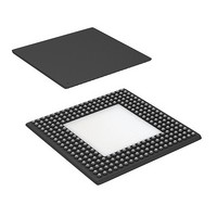
CYV15G0104TRB-BGXC Cypress Semiconductor Corp, CYV15G0104TRB-BGXC Datasheet - Page 7

CYV15G0104TRB-BGXC
Manufacturer Part Number
CYV15G0104TRB-BGXC
Description
IC SERDES HOTLINK 256LBGA
Manufacturer
Cypress Semiconductor Corp
Type
Serializer and Reclocking Deserializerr
Datasheet
1.CYV15G0104TRB-BGXC.pdf
(30 pages)
Specifications of CYV15G0104TRB-BGXC
Package / Case
256-LBGA Exposed Pad, 32-HLBGA
Function
Serializer/Deserializer
Data Rate
1.485Gbps
Input Type
PECL
Output Type
PECL
Number Of Inputs
2
Number Of Outputs
2
Voltage - Supply
3.15 V ~ 3.45 V
Operating Temperature
0°C ~ 70°C
Mounting Type
Surface Mount
Operating Supply Voltage
3.3 V
Supply Current
560 mA
Maximum Operating Temperature
+ 70 C
Minimum Operating Temperature
0 C
Mounting Style
SMD/SMT
Number Of Channels
2
Operating Supply Voltage (typ)
3.3V
Operating Supply Voltage (min)
3.13V
Operating Supply Voltage (max)
3.47V
Operating Temp Range
0C to 70C
Operating Temperature Classification
Commercial
Mounting
Surface Mount
Pin Count
256
Lead Free Status / RoHS Status
Lead free / RoHS Compliant
Lead Free Status / RoHS Status
Lead free / RoHS Compliant, Lead free / RoHS Compliant
Available stocks
Company
Part Number
Manufacturer
Quantity
Price
Company:
Part Number:
CYV15G0104TRB-BGXC
Manufacturer:
Cypress
Quantity:
568
Company:
Part Number:
CYV15G0104TRB-BGXC
Manufacturer:
CYPRESS
Quantity:
853
Company:
Part Number:
CYV15G0104TRB-BGXC
Manufacturer:
Cypress Semiconductor Corp
Quantity:
10 000
Document Number : 38-02100 Rev. *D
Pin Definitions
CYV15G0104TRB HOTLink II Serializer and Reclocking Deserializer
BISTSTA
REPDOA
TRGCLKA±
RXCLKA±
RECLKOA
RESET
LDTDEN
Name
Receive Path Clock Signals
Device Control Signals
LVTTL Output,
synchronous to the
RXCLKA ± output
Asynchronous to
reclocker output
channel
enable/disable
Differential LVPECL
or single-ended
LVTTL input clock
LVTTL Output Clock
LVTTL Output
LVTTL Input,
asynchronous,
internal pull-up
LVTTL Input,
internal pull-up
I/O Characteristics
(continued)
BIST Status Output. When RXBISTA[1:0] = 10, BISTSTA (along with RXDA[1:0])
displays the status of the BIST reception. See
each combination of BISTSTA and RXDA[1:0].
When RXBISTA[1:0] 10, BISTSTA should be ignored.
Reclocker Powered Down Status Output. REPDOA is asserted HIGH, when the
reclocker output logic is powered down. This occurs when ROE2A and ROE1A are both
disabled by setting ROE2A = 0 and ROE1A = 0.
CDR PLL Training Clock. TRGCLKA± clock inputs are used as the reference source for
the frequency detector (Range Controller) of the receive PLL to reduce PLL acquisition
time.
In the presence of valid serial data, the recovered clock output of the receive CDR PLL
(RXCLKA±) has no frequency or phase relationship with TRGCLKA±.
When driven by a single-ended LVCMOS or LVTTL clock source, connect the clock source
to either the true or complement TRGCLKA input, and leave the alternate TRGCLKA input
open (floating). When driven by an LVPECL clock source, the clock must be a differential
clock, using both inputs.
Receive Clock Output. RXCLKA± is the receive interface clock used to control timing of
the RXDA[9:0] parallel outputs. These true and complement clocks are used to control
timing of data output transfers. These clocks are output continuously at either the
half-character rate (1/20
the data being received, as selected by RXRATEA.
Reclocker Clock Output. RECLKOA output clock is synthesized by the reclocker output
PLL and operates synchronous to the internal recovered character clock. RECLKOA
operates at either the same frequency as RXCLKA± (RXRATEA = 0), or at twice the
frequency of RXCLKA± (RXRATEA = 1).The reclocker clock outputs have no fixed phase
relationship to RXCLKA±.
Asynchronous Device Reset. RESET initializes all state machines, counters, and
configuration latches in the device to a known state. RESET must be asserted LOW for a
minimum pulse width. When the reset is removed, all state machines, counters and config-
uration latches are at an initial state. As per the JTAG specifications the device RESET
cannot reset the JTAG controller. Therefore, the JTAG controller has to be reset
separately. Refer to
machine. See
latches.
Level Detect Transition Density Enable. When LDTDEN is HIGH, the Signal Level
Detector, Range Controller, and Transition Density Detector are all enabled to determine
if the RXPLL tracks TRGCLKA± or the selected input serial data stream. If the Signal Level
Detector, Range Controller, or Transition Density Detector are out of their respective limits
while LDTDEN is HIGH, the RXPLL locks to TRGCLKA± until such a time they become
valid. SDASEL[2..1]A[1:0] is used to configure the trip level of the Signal Level Detector.
The Transition Density Detector limit is one transition in every 60 consecutive bits. When
LDTDEN is LOW, only the Range Controller is used to determine if the RXPLL tracks
TRGCLKA± or the selected input serial data stream. it is recommended to set LDTDEN
= HIGH.
Signal Description
Table 4 on page 14
“JTAG Support” on page 16
th
the serial bit-rate) or character rate (1/10
for the initialize values of the device configuration
Table 6
for the methods to reset the JTAG state
for the BIST status reported for
CYV15G0104TRB
th
the serial bit-rate) of
Page 7 of 30
[+] Feedback


