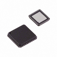
AD9949KCPZ Analog Devices Inc, AD9949KCPZ Datasheet - Page 26

AD9949KCPZ
Manufacturer Part Number
AD9949KCPZ
Description
IC CCD SIGNAL PROCESSOR 40-LFCSP
Manufacturer
Analog Devices Inc
Type
CCD Signal Processor, 12-Bitr
Datasheet
1.AD9949AKCPZ.pdf
(36 pages)
Specifications of AD9949KCPZ
Input Type
Logic
Output Type
Logic
Interface
3-Wire Serial
Mounting Type
Surface Mount
Package / Case
40-LFCSP
Analog Front End Type
CCD
Analog Front End Category
Video
Interface Type
Serial (3-Wire)
Sample Rate
36MSPS
Input Voltage Range
0.5V
Operating Supply Voltage (min)
2.7V
Operating Supply Voltage (typ)
3V
Operating Supply Voltage (max)
3.6V
Resolution
12b
Number Of Adc's
1
Power Supply Type
Analog/Digital
Operating Temp Range
-20C to 85C
Operating Temperature Classification
Commercial
Mounting
Surface Mount
Pin Count
40
Package Type
LFCSP EP
Number Of Channels
1
Lead Free Status / RoHS Status
Lead free / RoHS Compliant
Current - Supply
-
Lead Free Status / RoHS Status
Compliant, Lead free / RoHS Compliant
Available stocks
Company
Part Number
Manufacturer
Quantity
Price
Company:
Part Number:
AD9949KCPZ
Manufacturer:
TI
Quantity:
6 528
Part Number:
AD9949KCPZ
Manufacturer:
ADI/亚德诺
Quantity:
20 000
Company:
Part Number:
AD9949KCPZRL
Manufacturer:
PERICOM
Quantity:
3
AD9949
ANALOG FRONT END DESCRIPTION AND OPERATION
The AD9949 signal processing chain is shown in Figure 28.
Each processing step is essential in achieving a high quality
image from the raw CCD pixel data.
DC RESTORE
To reduce the large dc offset of the CCD output signal, a dc
restore circuit is used with an external 0.1 µF series coupling
capacitor. This restores the dc level of the CCD signal to
approximately 1.5 V to be compatible with the 3 V supply
voltage of the AD9949.
CORRELATED DOUBLE SAMPLER
The CDS circuit samples each CCD pixel twice to extract the
video information and reject low frequency noise. The timing
shown in Figure 17 illustrates how the two internally generated
CDS clocks, SHP and SHD, are used to sample the reference
level and the CCD signal level, respectively. The placement of
the SHP and SHD sampling edges is determined by the setting
of the SAMPCONTROL register located at Address 0×63.
Placement of these two clock signals is critical in achieving the
best performance from the CCD.
The gain in the CDS is fixed at 0 dB by default. Using Bits D10
and D11 in the AFE operation register, the gain may be reduced
to −2 dB or −4 dB. This allows the AD9949 to accept an input
signal of greater than 1 V p-p. See Table 14 for register details.
1.0µF
CCDIN
DC RESTORE
1.5V
0dB, –2dB, –4dB
SHP
CDS
SHD
SHP SHD
GENERATION
PRECISION
TIMING
REGISTERS
PxGA GAIN
PHASE
DOUT
0dB ~ 18dB
PxGA
Figure 28. Analog Front End Functional Block Diagram
CLPOB PBLK
GENERATION
REGISTER
TIMING
VGA GAIN
V-H
6dB ~ 42dB
VGA
Rev. B | Page 26 of 36
DAC
Table 22. Adjustable CDS Gain
D11
0
0
1
1
PxGA
The PxGA provides separate gain adjustment for the individual
color pixels. A programmable gain amplifier with four separate
values, the PxGA has the capability to multiplex its gain value
on a pixel-to-pixel basis (see Figure 29). This allows lower
output color pixels to be gained up to match higher output color
pixels. Also, the PxGA may be used to adjust the colors for
white balance, reducing the amount of digital processing that
is needed. The four different gain values are switched according
to the color steering circuitry. Three different color steering
modes for different types of CCD color filter arrays are
programmable in the AFE CTLMODE register at Address 0×03
(see Figure 33 to Figure 35 for timing examples). For example,
progressive steering mode accommodates the popular Bayer
arrangement of red, green, and blue filters (see Figure 30).
Operation Register Bits
DIGITAL
FILTER
OPTICAL BLACK
INTERNAL
CLAMP
REFB
1.0V
12-BIT
1.0µF 1.0µF
VREF
ADC
2V FULL SCALE
D10
0
1
0
1
REFT
2.0V
CLAMP LEVEL
REGISTER
8
CLPOB
OUTPUT
AD9949
LATCH
DATA
CDS Gain
0 dB
−2 dB
−4 dB
0 dB
PBLK
PHASE
DOUT
12
Max CDS Input
1.0 V p-p
1.2 V p-p
1.6 V p-p
1.0 V p-p
DOUT


