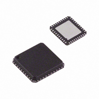
AD9949KCPZ Analog Devices Inc, AD9949KCPZ Datasheet - Page 25

AD9949KCPZ
Manufacturer Part Number
AD9949KCPZ
Description
IC CCD SIGNAL PROCESSOR 40-LFCSP
Manufacturer
Analog Devices Inc
Type
CCD Signal Processor, 12-Bitr
Datasheet
1.AD9949AKCPZ.pdf
(36 pages)
Specifications of AD9949KCPZ
Input Type
Logic
Output Type
Logic
Interface
3-Wire Serial
Mounting Type
Surface Mount
Package / Case
40-LFCSP
Analog Front End Type
CCD
Analog Front End Category
Video
Interface Type
Serial (3-Wire)
Sample Rate
36MSPS
Input Voltage Range
0.5V
Operating Supply Voltage (min)
2.7V
Operating Supply Voltage (typ)
3V
Operating Supply Voltage (max)
3.6V
Resolution
12b
Number Of Adc's
1
Power Supply Type
Analog/Digital
Operating Temp Range
-20C to 85C
Operating Temperature Classification
Commercial
Mounting
Surface Mount
Pin Count
40
Package Type
LFCSP EP
Number Of Channels
1
Lead Free Status / RoHS Status
Lead free / RoHS Compliant
Current - Supply
-
Lead Free Status / RoHS Status
Compliant, Lead free / RoHS Compliant
Available stocks
Company
Part Number
Manufacturer
Quantity
Price
Company:
Part Number:
AD9949KCPZ
Manufacturer:
TI
Quantity:
6 528
Part Number:
AD9949KCPZ
Manufacturer:
ADI/亚德诺
Quantity:
20 000
Company:
Part Number:
AD9949KCPZRL
Manufacturer:
PERICOM
Quantity:
3
POWER-UP PROCEDURE
RECOMMENDED POWER-UP SEQUENCE
When the AD9949 is powered up, the following sequence is
recommended (refer to Figure 27 for each step):
1.
2.
3.
4.
Turn on the power supplies for the AD9949.
Apply the master clock input, CLI, VD, and HD.
Although the AD9949 contains an on-chip, power-on reset,
a software reset of the internal registers is recommended.
Write a 1 to the SW_RST register (Address 0×10), which
resets the internal registers to their default values. This bit
is self-clearing and automatically resets back to 0.
The Precision Timing core must be reset by writing a 0 to
the TGCORE_RSTB register (Address 0×12) followed by
writing a l to the TGCORE_RSTB register. This starts the
internal timing core operation.
(OUTPUT)
(OUTPUT)
OUTPUTS
WRITES
DIGITAL
(INPUT)
(INPUT)
SERIAL
VDD
CLI
VD
HD
1
2
2
t
PWR
H1/H3, RG
H2/H4
3
4
...
...
5
Figure 27. Recommended Power-Up Sequence
6
Rev. B | Page 25 of 36
7
5.
6.
7.
8.
9.
8
9
Write a 1 to the PREVENTUPDATE register (Address
0×14). This prevents the updating of the serial register
data.
Write to the desired registers to configure high speed
timing and horizontal timing.
Write a 1 to the OUT_CONTROL register (Address 0×11).
This allows the outputs to become active after the next
VD/HD rising edge.
Write a 0 to the PREVENTUPDATE register (Address
0×14). This allows the serial information to be updated at
next VD/HD falling edge.
The next VD/HD falling edge allows register updates to
occur, including OUT_CONTROL, which enables all clock
outputs.
1H
ODD FIELD
CLOCKS ACTIVE WHEN OUT_CONTROL REGISTER IS
UPDATED AT VD/HD EDGE
1V
...
...
EVEN FIELD
AD9949


