AMIS49587C5872G ON Semiconductor, AMIS49587C5872G Datasheet - Page 5
AMIS49587C5872G
Manufacturer Part Number
AMIS49587C5872G
Description
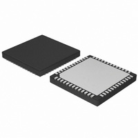
IC MODEM PLC 50/60MHZ 52QFN
Manufacturer
ON Semiconductor
Datasheet
1.AMIS49587C5871RG.pdf
(55 pages)
Specifications of AMIS49587C5872G
Baud Rates
Selectable
Interface
SCI
Voltage - Supply
3 V ~ 3.6 V
Mounting Type
Surface Mount
Package / Case
52-TQFN Exposed Pad
Maximum Operating Temperature
+ 80 C
Minimum Operating Temperature
- 40 C
Modulation Type
.
Mounting Style
SMD/SMT
Operating Supply Voltage
+ 3 V to 3.6 V
Number Of Transmitters
1
Power Supply Requirement
Single
Package Type
QFN EP
Operating Temperature Classification
Commercial
Mounting
Surface Mount
Pin Count
52
Operating Temperature (min)
-40C
Dual Supply Voltage (typ)
Not RequiredV
Dual Supply Voltage (max)
Not RequiredV
Dual Supply Voltage (min)
Not RequiredV
Lead Free Status / RoHS Status
Lead free / RoHS Compliant
Data Format
-
Lead Free Status / Rohs Status
Compliant


3.1 PLCC Packaging
Table 6. AMIS- -49587 PLCC PIN FUNCTION DESCRIPTION
P:
A:
D:
Pin No.
10
11
12
13
14
15
16
17
18
19
20
21
22
23
24
25
26
27
28
1
2
3
4
5
6
7
8
9
Power pin
Analog pin
Digital pin
PRE_SLOT
M50HZ_IN
REF_OUT
TX_DATA/
Pin Name
RX_DATA
RX_OUT
TX_ENB
TX_OUT
ALC_IN
TRSTB
T_REQ
RX_IN
VSSA
XOUT
RESB
VDDA
TEST
TDO
TMS
VDD
RXD
CRC
TCK
VSS
TXD
BR1
BR0
TDI
XIN
Out
Out
Out
Out
Out
Out
Out
Out
Out
Out
I/O
In
In
In
In
In
In
In
In
In
In
In
In
In
In
M50Hz_IN
RX_DATA
TRSTB
TDO
TMS
TCK
TDI
D, 5V Safe
D, 5V Safe
D, 5V Safe
D, 5V Safe
D, 5V Safe
D, 5V Safe
D, 5V Safe
D, 5V Safe
D, 5V Safe
D, 5V Safe
10
11
5
6
7
8
9
Type
P
A
A
A
A
D
D
D
D
D
A
A
P
P
D
A
A
P
3 PIN DESCRIPTION
http://onsemi.com
Figure 2. Pinout
12 13 14 15 16 17 18
4
3
AMIS- -49587
Analog ground
Output of receiver low noise operational amplifier
Positive input of receiver low noise operational amplifier
Reference output for stabilization
50/60 Hz input for mains zero cross detection
Data reception indication (open drain output)
Test data output
Test data input (internal pulldown)
Test clock (internal pulldown)
Test mode select (internal pulldown)
Test reset bar (internal pulldown, active low)
Data output corresponding to transmitted data or PRE_SLOT signal
(open drain output)
Xtal input (can be driven by an internal clock)
Xtal output (output floating when XIN driven by external clock)
Digital ground
3.3 V digital supply
SCI transmit output (open drain)
SCI receive input (Schmitt trigger input)
Transmit request input
SCI baud rate selection
SCI baud rate selection
Correct frame CRC indication (open drain output)
Master reset bar (Schmitt trigger input, active low)
Test enable (internal pulldown)
TX enable bar (open drain)
Transmitter output
Automatic level control input
3.3 V analog supply
5V Safe: IO that support the presence of 5V on bus line
Out:
In:
In/Out:
2
5
1 28 27 26
Output signal
Input signal
Bi--directional pin
25
24
23
22
21
20
19
TX _ENB
TEST
RESB
CRC
BR0
BR1
T_REQ
Description
Related parts for AMIS49587C5872G
Image
Part Number
Description
Manufacturer
Datasheet
Request
R

Part Number:
Description:
ON Semiconductor [VOLTAGE REGULATOR]
Manufacturer:
ON Semiconductor
Datasheet:
Part Number:
Description:
357-036-542-201 CARDEDGE 36POS DL .156 BLK LOPRO
Manufacturer:
ON Semiconductor
Datasheet:
Part Number:
Description:
357-036-542-201 CARDEDGE 36POS DL .156 BLK LOPRO
Manufacturer:
ON Semiconductor
Datasheet:
Part Number:
Description:
357-036-542-201 CARDEDGE 36POS DL .156 BLK LOPRO
Manufacturer:
ON Semiconductor
Datasheet:
Part Number:
Description:
357-036-542-201 CARDEDGE 36POS DL .156 BLK LOPRO
Manufacturer:
ON Semiconductor
Datasheet:
Part Number:
Description:
357-036-542-201 CARDEDGE 36POS DL .156 BLK LOPRO
Manufacturer:
ON Semiconductor
Datasheet:
Part Number:
Description:
357-036-542-201 CARDEDGE 36POS DL .156 BLK LOPRO
Manufacturer:
ON Semiconductor
Datasheet:
Part Number:
Description:
357-036-542-201 CARDEDGE 36POS DL .156 BLK LOPRO
Manufacturer:
ON Semiconductor
Datasheet:
Part Number:
Description:
357-036-542-201 CARDEDGE 36POS DL .156 BLK LOPRO
Manufacturer:
ON Semiconductor
Datasheet:
Part Number:
Description:
357-036-542-201 CARDEDGE 36POS DL .156 BLK LOPRO
Manufacturer:
ON Semiconductor
Datasheet:
Part Number:
Description:
357-036-542-201 CARDEDGE 36POS DL .156 BLK LOPRO
Manufacturer:
ON Semiconductor
Datasheet:
Part Number:
Description:
Manufacturer:
ON Semiconductor
Datasheet:
Part Number:
Description:
Manufacturer:
ON Semiconductor
Datasheet:
Part Number:
Description:
Manufacturer:
ON Semiconductor
Datasheet: