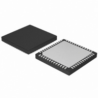
AMIS49587C5872G ON Semiconductor, AMIS49587C5872G Datasheet - Page 25

AMIS49587C5872G
Manufacturer Part Number
AMIS49587C5872G
Description
IC MODEM PLC 50/60MHZ 52QFN
Manufacturer
ON Semiconductor
Datasheet
1.AMIS49587C5871RG.pdf
(55 pages)
Specifications of AMIS49587C5872G
Baud Rates
Selectable
Interface
SCI
Voltage - Supply
3 V ~ 3.6 V
Mounting Type
Surface Mount
Package / Case
52-TQFN Exposed Pad
Maximum Operating Temperature
+ 80 C
Minimum Operating Temperature
- 40 C
Modulation Type
.
Mounting Style
SMD/SMT
Operating Supply Voltage
+ 3 V to 3.6 V
Number Of Transmitters
1
Power Supply Requirement
Single
Package Type
QFN EP
Operating Temperature Classification
Commercial
Mounting
Surface Mount
Pin Count
52
Operating Temperature (min)
-40C
Dual Supply Voltage (typ)
Not RequiredV
Dual Supply Voltage (max)
Not RequiredV
Dual Supply Voltage (min)
Not RequiredV
Lead Free Status / RoHS Status
Lead free / RoHS Compliant
Data Format
-
Lead Free Status / Rohs Status
Compliant
6.3.2 50/60 Hz Suppression Filter
operational amplifier in a follower configuration which can
be used to make a 50/60 Hz suppression filter with a
noise input op- -amp. Together with the output RX_OUT an
active high pass filter is realized. This filter removes the
main frequency (50 Hz or 60 Hz) from the received signal.
The filter characteristics are determined by external
capacitors and resistors. Typical values are given in
Table 26. For these values and after this filter, a typical
voltage reference used by the A/D converter. This pin must
be decoupled from the analog ground by a 1 mF ceramic
capacitance (C
powered down by setting the bit R_RX_MOD[7] to 1. In
this mode the pin RX_OUT must be used as input of the
AGC.
AMIS- -49587 receiver input provides a low noise input
RX_IN is the positive analog input pin of the receiver low
REF_OUT is the analog output pin which provides the
The low noise operational amplifier can be bypassed and
Received
Signal
DREF
). It is not allowed to load this pin.
Figure 21. External Component Connection for 50/60 Hz Suppression Filter
--100
--140
--20
--60
20
C
2
10
Figure 22. Transfer Function of 50 Hz Suppression Circuit
C
V
DREF
SSA
R
C
2
1
R
1
REF_OUT
RX_OUT
RX_IN
100
2
4
3
http://onsemi.com
Frequency (Hz)
LOW NOISE
25
OPAMP
1, 65 V
1k
minimum number of external components. Pin RX_IN is
the positive input and RX_OUT is the output of the input
low noise operational amplifier. The pin REF_OUT can be
use as an analog ground (1.65 V) for the external circuitry.
attenuation of 85 dB at 50 Hz is obtained. Figure 21
represents external components connection. In a typical
application the coupling transformer in combination with a
parallel capacitance forms a high pass filter with a typical
attenuation of 60 dB. The combined effect of the two filters
decreases the voltage level of 230 Vrms at the mains
frequency well below the sensitivity of the AMIS- -49587.
REF
TO AGC
Receiver (S-- FSK Demodulator)
10k
100k


