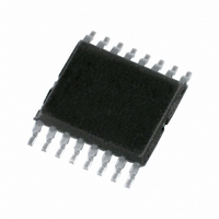
PCA9500PW,112 NXP Semiconductors, PCA9500PW,112 Datasheet - Page 6

PCA9500PW,112
Manufacturer Part Number
PCA9500PW,112
Description
IC I/O EXPANDER I2C 8B 16TSSOP
Manufacturer
NXP Semiconductors
Datasheet
1.PCA9500BS118.pdf
(26 pages)
Specifications of PCA9500PW,112
Package / Case
16-TSSOP
Interface
I²C, SMBus
Number Of I /o
8
Interrupt Output
No
Frequency - Clock
400kHz
Voltage - Supply
2.5 V ~ 3.6 V
Operating Temperature
-40°C ~ 85°C
Mounting Type
Surface Mount
Includes
EEPROM, POR
Logic Family
PCA9500
Number Of Lines (input / Output)
8.0 / 8.0
Operating Supply Voltage
2.5 V to 3.6 V
Power Dissipation
400 mW
Operating Temperature Range
- 40 C to + 85 C
Input Voltage
5 V
Logic Type
I/O Expander
Maximum Clock Frequency
400 KHz
Mounting Style
SMD/SMT
Number Of Input Lines
8.0
Number Of Output Lines
8.0
Output Current
25 mA
Output Voltage
5 V
Operating Temperature (min)
-40C
Operating Temperature Classification
Industrial
Operating Temperature (max)
85C
Package Type
TSSOP
Rad Hardened
No
Lead Free Status / RoHS Status
Lead free / RoHS Compliant
Lead Free Status / RoHS Status
Lead free / RoHS Compliant, Lead free / RoHS Compliant
Other names
568-1025-5
935271534112
PCA9500PW
935271534112
PCA9500PW
NXP Semiconductors
PCA9500_4
Product data sheet
Fig 7.
Fig 8.
read from
data into
SDA
port
port
write to port
data out from port
I/O Write mode (output)
I/O Read mode (input)
SCL
S
START condition
SDA
slave address (I/O expander)
SCL
1
0
7.3 I/O operations
S
START condition
2
1
slave address (I/O expander)
1
0
3
0
(Refer also to
Each of the PCA9500's eight I/Os can be independently used as an input or output.
Output data is transmitted to the port by the I/O Write mode (see
is transferred from the port to the microcontroller by the Read mode (see
2
1
4
0 A2 A1 A0
3
0
DATA 1
5
4
0 A2 A1 A0 1
6
5
7
R/W
6
8
0
Figure
7
t
9
h(D)
A
acknowledge
from slave
R/W
8
9
5.)
A
acknowledge
from slave
Rev. 04 — 15 April 2009
data to port
DATA 1
DATA 2
data from port
8-bit I
DATA 1
DATA 3
t
v(Q)
t
su(D)
2
C-bus and SMBus I/O port with 2-kbit EEPROM
A
acknowledge
from slave
A
acknowledge
from master
data to port
DATA 1 VALID
DATA 2
data from port
DATA 4
DATA 4
t
v(Q)
Figure
A
acknowledge
from slave
PCA9500
© NXP B.V. 2009. All rights reserved.
DATA 2 VALID
7). Input I/O data
Figure
1
no acknowledge
from master
002aae591
002aae592
P
STOP
condition
8).
6 of 26


