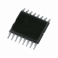
PCA9500PW,112 NXP Semiconductors, PCA9500PW,112 Datasheet - Page 5

PCA9500PW,112
Manufacturer Part Number
PCA9500PW,112
Description
IC I/O EXPANDER I2C 8B 16TSSOP
Manufacturer
NXP Semiconductors
Datasheet
1.PCA9500BS118.pdf
(26 pages)
Specifications of PCA9500PW,112
Package / Case
16-TSSOP
Interface
I²C, SMBus
Number Of I /o
8
Interrupt Output
No
Frequency - Clock
400kHz
Voltage - Supply
2.5 V ~ 3.6 V
Operating Temperature
-40°C ~ 85°C
Mounting Type
Surface Mount
Includes
EEPROM, POR
Logic Family
PCA9500
Number Of Lines (input / Output)
8.0 / 8.0
Operating Supply Voltage
2.5 V to 3.6 V
Power Dissipation
400 mW
Operating Temperature Range
- 40 C to + 85 C
Input Voltage
5 V
Logic Type
I/O Expander
Maximum Clock Frequency
400 KHz
Mounting Style
SMD/SMT
Number Of Input Lines
8.0
Number Of Output Lines
8.0
Output Current
25 mA
Output Voltage
5 V
Operating Temperature (min)
-40C
Operating Temperature Classification
Industrial
Operating Temperature (max)
85C
Package Type
TSSOP
Rad Hardened
No
Lead Free Status / RoHS Status
Lead free / RoHS Compliant
Lead Free Status / RoHS Status
Lead free / RoHS Compliant, Lead free / RoHS Compliant
Other names
568-1025-5
935271534112
PCA9500PW
935271534112
PCA9500PW
NXP Semiconductors
7. Functional description
PCA9500_4
Product data sheet
7.1 Device addressing
7.2 Control register
Refer also to
Following a START condition, the bus master must output the address of the slave it is
accessing. The address of the PCA9500 is shown in
are incorporated on the hardware selectable address pins.
The last bit of the address byte defines the operation to be performed. When set to logic 1
a read is selected, while a logic 0 selects a write operation.
The PCA9500 contains a single 8-bit register called the Control register, which can be
written and read via the I
of the slave address. It contains the I/O operation information.
Fig 5.
Fig 6.
data from shift register
a. I/O expander
data to shift register
0
Simplified schematic diagram of each I/O
PCA9500 slave addresses
power-on reset
1
fixed
Figure 1 “Block diagram of
write pulse
read pulse
slave address
0
0
programmable
A2
Rev. 04 — 15 April 2009
hardware
2
C-bus. This register is sent after a successful acknowledgment
A1
002aae589
A0 R/W
D
CI
8-bit I
FF
S
Q
2
C-bus and SMBus I/O port with 2-kbit EEPROM
PCA9500”.
D
CI
FF
S
Q
b. Memory
Figure
1
100 A
0
fixed
6. Internal pull-up resistors
slave address
1
002aae588
0
programmable
A2
hardware
PCA9500
© NXP B.V. 2009. All rights reserved.
A1
V
IO0 to IO7
V
to interrupt logic
DD
SS
002aae590
A0 R/W
5 of 26


