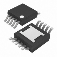
MAX7430EUB+T Maxim Integrated Products, MAX7430EUB+T Datasheet - Page 12

MAX7430EUB+T
Manufacturer Part Number
MAX7430EUB+T
Description
IC FILTER VIDEO SD 10-UMAX
Manufacturer
Maxim Integrated Products
Datasheet
1.MAX7432EUDT.pdf
(21 pages)
Specifications of MAX7430EUB+T
Filter Type
Low Pass
Frequency - Cutoff Or Center
5MHz
Number Of Filters
2
Max-order
6th
Voltage - Supply
4.5 V ~ 5.5 V
Mounting Type
Surface Mount
Package / Case
10-MSOP Exposed Pad, 10-HMSOP, 10-eMSOP
Lead Free Status / RoHS Status
Lead free / RoHS Compliant
Table 7. Initialization Capacitor Values and Pulse Widths
(C
An address sequence precedes a write or read opera-
tion to determine with which device to communicate. If
the address transmitted in this mode matches with a
device’s address, the device and µP can initiate data
transfer. When entering the four address bits, ensure
that the LSB is entered first. The following is the com-
mand sequence and timing diagram (Figure 6) for an
address sequence.
Use a write sequence to load data into the data register
of the device. It must follow an address sequence.
Transmit a minimum of eight data bits for the MAX7428,
16 data bits for the MAX7430, or 24 data bits for the
MAX7432A to make this transaction valid starting with
the LSB first. The last 8/16/24 data bits are used if more
Standard Definition Video Reconstruction
Filters and Buffers
Note: ( ) Indicates the time periods associated with 20% capacitors. This limits the maximum number of devices on the bus to seven.
12
Initialize wait
Initialization Command Sequence:
CAPACITOR VALUE (nF)
REXT
Address Command Sequence:
______________________________________________________________________________________
T010
= ±10% Tolerance, R
1000
680
470
220
150
100
6.8
4.7
2.2
1.5
68
47
22
15
10
1
T011
MAX7428/MAX7430/MAX7432A
Initialize Time Address ID = 4-bits
Address = 4-bits
INITIALIZING WAIT PERIOD
Programming the
(ms) (t
REXT
20.000
13.600
9.400
4.400
3.000
2.000
1.360
0.940
0.440
0.300
0.200
0.136
0.094
0.044
0.030
0.020
INTWAIT
= ±1% Tolerance)
T111
)
T111
than 8/16/24 bits are loaded into the register. The fol-
lowing is the command sequence and timing diagram
(Figure 7) for a write sequence.
During the read sequence, the µP sends a prompt
pulse causing the device to output the data word LSB
first. Similar to the write transaction, the read transac-
tion must be preceded by an address sequence. If
more than 8 prompts (MAX7428), 16 prompts
(MAX7430), or 24 prompts (MAX7432A) are available,
the device outputs the same data starting with the LSB
again. The following is the command sequence and
timing diagram (Figure 8) for a read sequence.
0.526 (0.441)
0.162 (0.137)
23.90 (13.7)
1.625 (1.37)
162 (136.8)
Write Command Sequence:
52.6 (44.1)
11.21 (4.4)
35.90
16.25
1.121
0.359
0.239
MIN
5.26
3.59
2.39
112
T001
INITIALIZING TIME PERIOD (ms)
WITH R
Data ≥ 8-bits (MAX7428,
See Table 1)
Data ≥ 16-bits (MAX7430,
See Table 3)
Data ≥ 24-bits (MAX7432A,
See Table 5)
0.554 (0.464)
0.171 (0.144)
REXT
25.20 (14.4)
11.80 (4.64)
1.710 (1.44)
55.4 (46.4)
171 (144)
1.180
0.378
0.252
37.80
17.10
TYP
5.54
3.78
2.52
118
= 300kΩ (t
INT
)
0.582 (0.487)
0.179 (0.151)
58.2 (48.72)
26.50 (15.1)
1.795 (1.51)
179 (151.2)
12.39 (4.9)
39.70
17.95
1.239
0.397
0.265
MAX
5.82
3.97
2.65
123
T111


