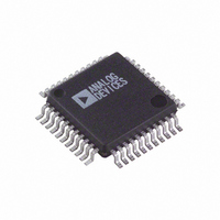
ADV7177KS-REEL Analog Devices Inc, ADV7177KS-REEL Datasheet - Page 30

ADV7177KS-REEL
Manufacturer Part Number
ADV7177KS-REEL
Description
IC DAC VIDEO NTSC 3-CH 44MQFP
Manufacturer
Analog Devices Inc
Type
Video Encoderr
Datasheet
1.ADV7177KSZ-REEL.pdf
(44 pages)
Specifications of ADV7177KS-REEL
Rohs Status
RoHS non-compliant
Applications
Set-Top Boxes, TV
Voltage - Supply, Analog
3 V ~ 3.6 V
Mounting Type
Surface Mount
Package / Case
44-MQFP, 44-PQFP
Adc/dac Resolution
9b
Screening Level
Commercial
Package Type
MQFP
Pin Count
44
Voltage - Supply, Digital
-
Lead Free Status / RoHS Status
Not Compliant
ADV7177/ADV7178
TIMING REGISTER 1 (TR17–TR10)
Address [SR4–SR0] = 0CH
Timing Register 1 is an 8-bit-wide register. Figure 38 shows the
various operations under the control of Timing Register 1. This
register can be read from as well as written to. This register can
be used to adjust the width and position of the master mode
timing signals.
TR1 BIT DESCRIPTION
HSYNC Width (TR11–TR10)
These bits adjust the HSYNC pulse width.
HSYNC to FIELD/ VSYNC Delay (TR13–TR12)
These bits adjust the position of the HSYNC output relative to
the FIELD/ VSYNC output.
HSYNC to FIELD Rising Edge Delay (TR15–TR14)
When the device is in Timing Mode 1, these bits adjust the
position of the HSYNC output relative to the FIELD output
rising edge.
TIMING MODE 1 (MASTER/PAL)
FIELD/VSYNC
MR27
TR17
LOW POWER
0
1
0
0
1
1
HSYNC TO PIXEL
DATA ADJUST
MODE
HSYNC
MR27
TR16
DISABLE
ENABLE
TR17
0
1
0
1
MR26
0
1
0 3 T
1 3 T
2 3 T
3 3 T
CONTROL
RGB/YUV
RGB OUTPUT
YUV OUTPUT
PCLK
PCLK
PCLK
PCLK
MR26
TR16
T
MR25
LINE 1
B
T
0
1
A
TR15
CONTROL
TR15
ENABLE BURST
DISABLE BURST
0
0
1
1
RISING EDGE DELAY
BURST
X
x
HSYNC TO FIELD
(MODE 2 ONLY)
VSYNC WIDTH
MR25
TR15
(MODE 1 ONLY)
TR14
TR14
0
1
0
1
MR24
0
1
0
1
CHROMINANCE
1 × T
4 × T
16 × T
128 × T
T
T
CONTROL
Figure 38. Timing Register 1
ENABLE COLOR
DISABLE COLOR
B
B
Figure 39. Mode Register 2
TR14
+ 32µs
T
PCLK
PCLK
MR24
PCLK
C
Rev. C | Page 30 of 44
PCLK
MR23
0
1
TR13
720 PIXELS
710 PIXELS/702 PIXELS
LINE DURATION
TR13
FIELD/VSYNC DELAY
ACTIVE VIDEO
0
0
1
1
MR23
TR12
HSYNC TO
VSYNC Width (TR15–TR14)
When the ADV7177/ADV7178 are in Timing Mode 2, these
bits adjust the VSYNC pulse width.
HSYNC to Pixel Data Adjust (TR17–TR16)
This enables the HSYNC to be adjusted with respect to the pixel
data and allows the Cr and Cb components to be swapped. This
adjustment is available in both master and slave timing modes.
MODE REGISTER 2 MR2 (MR27–MR20)
Address [SR4-SR0] = 0DH
Mode Register 2 is an 8-bit-wide register. Figure 39 shows the
various operations under the control of Mode Register 2. This
register can be read from as well as written to.
0
1
0
1
0 × T
4 × T
8 × T
16 × T
TR12
MR22
T
T
PCLK
PCLK
PCLK
BE WRITTEN TO
B
ZERO SHOULD
C
PCLK
MR22–MR21
THESE BITS
LINE 313
(00)
TR11
MR21
TR11
0
0
1
1
HSYNC WIDTH
TR10
LINE 314
0
1
0
1
MR20
TR10
SQUARE PIXEL
0
1
MR20
1 × T
4 × T
16 × T
128 × T
CONTROL
DISABLE
ENABLE
T
PCLK
PCLK
A
PCLK
PCLK


